
Electric current driving type display device

a display device and electric current technology, applied in semiconductor devices, electric discharge tubes, instruments, etc., can solve the problems of difficult to achieve a large-area circuit, difficult to suppress variations in luminance of organic el elements, and difficult to design pixel circuits and drive circuits, so as to achieve the effect of enhancing display quality and properly keeping luminance of electro-optical elements

Active Publication Date: 2012-12-04
SHARP KK
View PDF19 Cites 10 Cited by
  • Summary
  • Abstract
  • Description
  • Claims
  • Application Information

AI Technical Summary

Benefits of technology

[0068]According to the first or second aspect of the present invention, by applying a potential that brings the drive element into a conduction state to the third power supply wiring line and controlling the fourth switching element (or the third and fourth switching elements) to a conduction state, a potential of the third power supply wiring line is provided to the control terminal of the drive element and regardless of a previous state of the pixel circuit, the drive element can be surely set to a conduction state. Thus, when the third switching element is controlled to a conduction state, the drive element is reliably set to a threshold state (a state in which a threshold voltage is applied) and thus variations in the threshold voltage of the drive element can be properly compensated for.
[0069]According to the third aspect of the present invention, since the fourth switching element is provided between the third power supply wiring line and the control terminal of the drive element, by controlling the fourth switching element to a conduction state, a potential of the third power supply wiring line can be provided to the control terminal of the drive element.
[0070]According to the fourth aspect of the present invention, during the first period, a potential of the third power supply wiring line is provided to the first electrode of the capacitor, a potential according to display data (hereinafter, also referred to as a data potential) is provided to the second electrode of the capacitor, and a difference between these two potentials is held in the capacitor. During the second period, the potential of the first electrode of the capacitor changes until the drive element goes into a threshold state, and accordingly, the potential difference held in the capacitor is changed to a difference between the data potential and the threshold voltage of the drive element. During the third period, with the capacitor holding the above-described potential difference, the potential of the second electrode of the capacitor is changed from the data potential to a potential of a predetermined power supply wiring line. Thus, the control terminal potential of the drive element after that is a potential obtained by adding a difference between the potential of the predetermined power supply wiring line and the data potential to a potential at which the drive element goes into a threshold state. Therefore, even when the threshold voltage is different, if the data potential is the same, then the amount of current flowing through the drive element is the same. In this manner, variations in the threshold voltage of the drive element can be compensated for.
[0071]According to the fifth aspect of the present invention, since the fourth switching element is provided between the third power supply wiring line and the current input / output terminal of the drive element and the terminal is connected to the third switching element, by controlling both the third and fourth switching elements to a conduction state, a potential of the third power supply wiring line can be provided to the control terminal of the drive element. Also, since the control terminal of the drive element is connected to the third power supply wiring line through the third and fourth switching elements, the number of switching elements connected to the control terminal of the drive element is smaller than the case in which the control terminal of the drive element is connected to the third power supply wiring line through the fourth switching element. Therefore, the control terminal potential of the drive element is less likely to fluctuate due to a less amount of leakage current flowing through a switching element. Thus, the luminance of the electro-optical element can be properly kept and display quality can be enhanced.
[0072]According to the sixth aspect of the present invention, during the first period, a potential of the third power supply wiring line is provided to the first electrode of the capacitor, a data potential is provided to the second electrode of the capacitor, and a difference between these two potentials is held in the capacitor. During the second period, the potential of the first electrode of the capacitor changes until the drive element goes into a threshold state, and accordingly, the potential difference held in the capacitor is changed to a difference between the data potential and the threshold voltage of the drive element. During the third period, with the capacitor holding the above-described potential difference, the potential of the second electrode of the capacitor is changed from the data potential to a potential of a predetermined power supply wiring line. Thus, the control terminal potential of the drive element after that is a potential obtained by adding a difference between the potential of the predetermined power supply wiring line and the data potential to a potential at which the drive element goes into a threshold state. Therefore, even when the threshold voltage is different, if the data potential is the same, then the amount of current flowing through the drive element is the same. In this manner, variations in the threshold voltage of the drive element can be compensated for.
[0073]According to the seventh aspect of the present invention, by controlling the second switching element to a conduction state, a potential of the first power supply wiring line can be provided to the second electrode of the capacitor. Hence, the potential of the control terminal of the drive element which is connected to the first electrode of the capacitor can be kept at a level according to display data.

Problems solved by technology

Hence, when a voltage control type drive scheme is adopted in an organic EL display, it is very difficult to suppress variations in the luminance of the organic EL element.
However, the electric current program scheme has the following problems: first, since a very small amount of current is handled, it is difficult to design a pixel circuit and a drive circuit; and second, since it is susceptible to parasitic capacitance while a current signal is set, it is difficult to achieve a large-area circuit.

Method used


Image

  • Electric current driving type display device
  • Electric current driving type display device
  • Electric current driving type display device

Examples


first embodiment

[0135](First Embodiment)

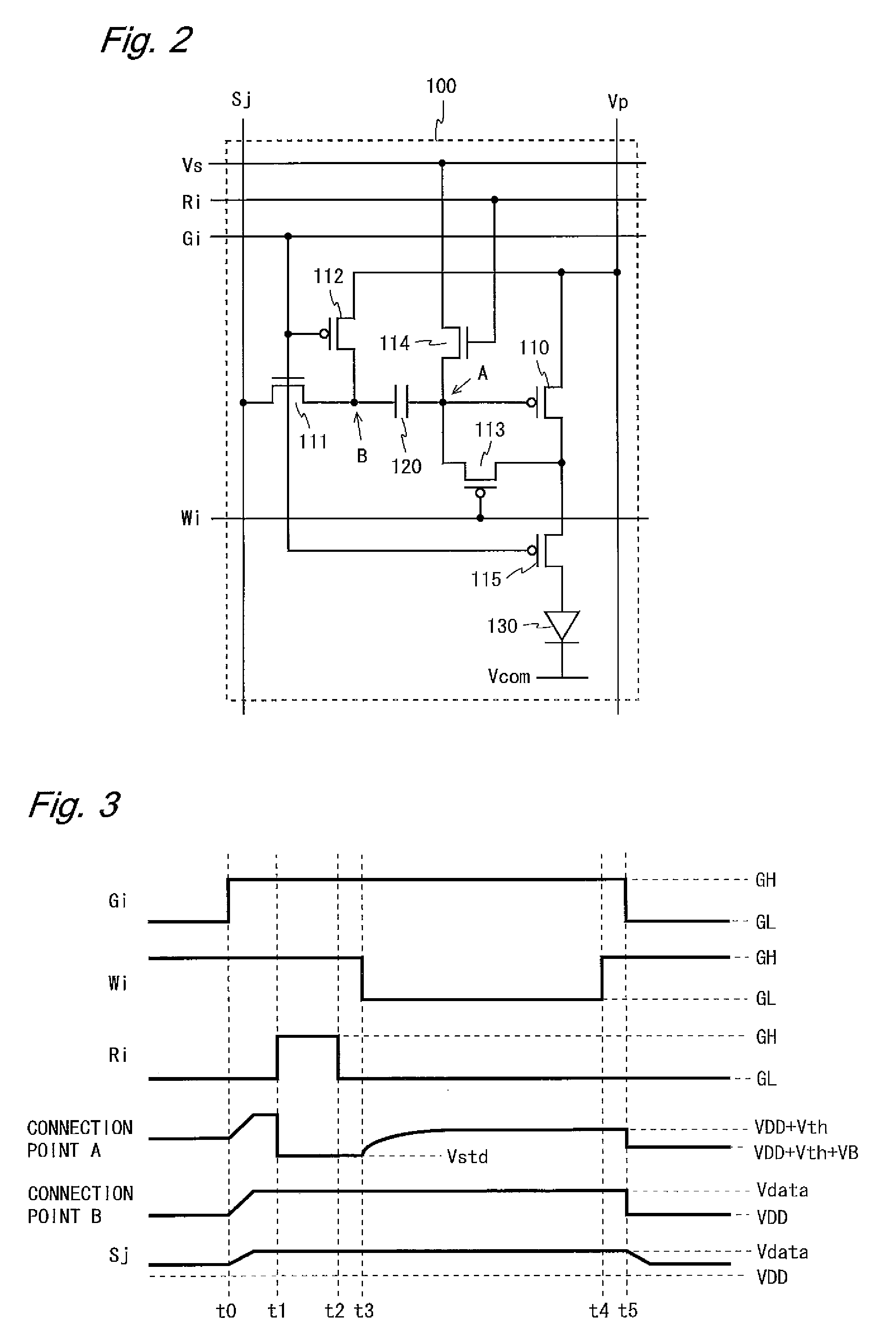
[0136]FIG. 2 is a circuit diagram of a pixel circuit included in a display device according to the first embodiment of the present invention, A pixel circuit 100 shown in FIG. 2 includes a driving TFT 110, switching TFTs 111 to 115, a capacitor 120, and an organic EL element 130. The switching TFTs 111 and 114 are of an n-channel type and other TFTs are of a p-channel type.

[0137]The pixel circuit 100 is connected to a power supply wiring line Vp, a reference supply wiring line Vs, a common cathode Vcom, a scanning line Gi, control lines Wi and Ri, and a data line Sj. Of them, to the power supply wiring line Vp (first power supply wiring line) and the common cathode Vcom (second power supply wiring line) are respectively applied fixed potentials VDD and VSS and to the reference supply wiring line Vs (third power supply wiring line) is applied a reference potential Vstd obtained by the reference supply adjustment circuit 14. The common cathode Vcom serves as a ...

second embodiment

[0159](Second Embodiment)

[0160]FIG. 4 is a circuit diagram of a pixel circuit included in a display device according to the second embodiment of the present invention. A pixel circuit 200 shown in FIG. 4 includes a driving TFT 210, switching TFTs 211 to 214, a capacitor 220, and an organic EL element 230. The switching TFTs 211 and 214 are of an n-channel type and other TFTs are of a p-channel type.

[0161]The pixel circuit 200 is obtained by making a change to the pixel circuit 100 (FIG. 2) according to the first embodiment such that the switching TFT 115 is eliminated and a cathode terminal of the organic EL element 130 is connected to a cathode wiring line CAi (second power supply wiring line). In the pixel circuit 200, on a path connecting a power supply wiring line Vp to the cathode wiring line CAi, in order from the side of the power supply wiring line Vp, the driving TFT 210 and the organic EL element 230 are provided in series. Except for the above points, the configuration of...

third embodiment

[0165](Third Embodiment)

[0166]FIG. 6 is a circuit diagram of a pixel circuit included in a display device according to the third embodiment of the present invention. A pixel circuit 300 shown in FIG. 6 includes a driving TFT 310, switching TFTs 311 to 315, a capacitor 320, and an organic EL element 330. All of the TFTs included in the pixel circuit 300 are of a p-channel type.

[0167]The pixel circuit 300 is obtained by making a change to the pixel circuit 100 (FIG. 2) according to the first embodiment such that the TFTs of an n-channel type are changed to TFT of a p-channel type and a gate terminal of each TFT is connected to an appropriate signal line. In the pixel circuit 300, gate terminals of the respective switching TFTs 311 and 313 are connected to a scanning line Gi, gate terminals of the respective switching TFTs 312 and 315 are connected to a control line Ei, and a gate terminal of the switching TFT 314 is connected to a control line Ri. Except for the above points, the conf...


PUM


Abstract

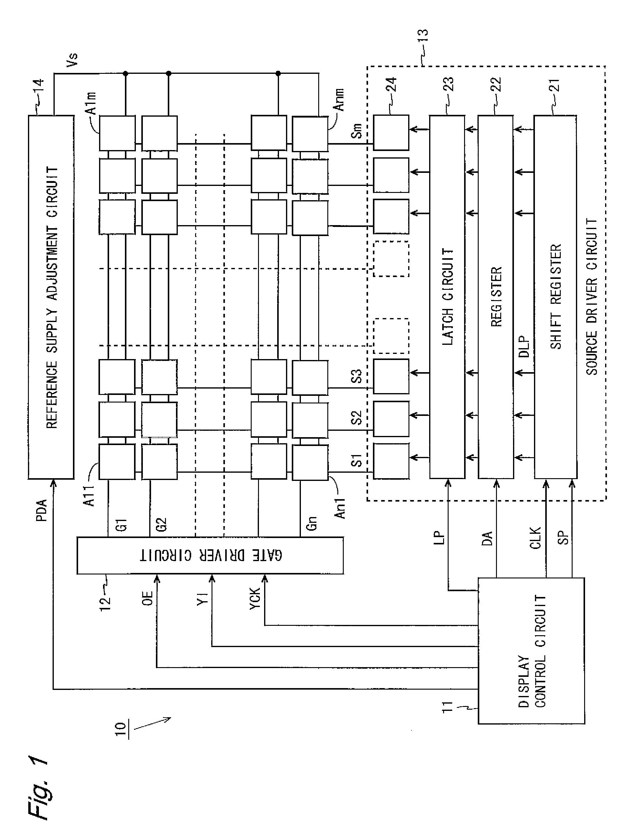
In a pixel circuit 100, a driving TFT 110, a switching TFT 115, and an organic EL element 130 are provided between a power supply wiring line Vp and a common cathode Vcom and a capacitor 120 and a switching TFT 111 are provided between a gate terminal of the driving TFT 110 and a data line Sj. A switching TFT 112 is provided between a connection point B between the capacitor 120 and the switching TFT 111 and the power supply wiring line Vp, a switching TFT 113 is provided between the gate and drain terminals of the driving TFT 110, and a switching TFT 114 is provided between the gate terminal of the driving TFT 110 and a reference supply wiring line Vs. A potential that brings the driving TFT 110 into a conduction state is applied to the reference supply wiring line Vs. Thus, variations in the threshold voltage of a drive element can be properly compensated for and unwanted light emission from an electro-optical element can be prevented.

Description

TECHNICAL FIELD[0001]The present invention relates to a display device and more particularly to an electric current driving type display device such as an organic EL display or FED.BACKGROUND ART[0002]In recent years, there have been demands for thin, lightweight, fast response display devices, and accordingly, research and development for organic EL (Electro Luminescence) displays and FEDs (Field Emission Displays) have been actively conducted.[0003]An organic EL element included in an organic EL display emits light with higher luminance as the voltage to be applied thereto is higher and the amount of current flowing therethrough is larger. However, the relationship between luminance and voltage of the organic EL element easily varies due to an influence such as drive time or ambient temperature. Hence, when a voltage control type drive scheme is adopted in an organic EL display, it is very difficult to suppress variations in the luminance of the organic EL element. In contrast to ...

Claims


Application Information

Patent Timeline
Patent Type & Authority Patents(United States)
IPC IPC(8): G09G3/36
CPCG09G3/3233G09G2300/0819G09G2300/0842G09G2300/0852G09G2320/043H01L27/3244G09G2300/0861H10K59/12
Inventor SENDA, TAKAHIRO
Owner SHARP KK
Learn More