Semiconductor device, display device, and electronic device

a technology of semiconductor devices and display devices, applied in static indicating devices, instruments, electroluminescent light sources, etc., can solve the problems of increase of voltage applied to light emitting elements and power consumption, and easy deterioration of light emitting elements or drive transistors. , to achieve the effect of suppressing the current value caused by the threshold voltage variation of transistors, less luminance variation, and high duty ratio

Active Publication Date: 2012-12-04
SEMICON ENERGY LAB CO LTD
View PDF56 Cites 30 Cited by
  • Summary
  • Abstract
  • Description
  • Claims
  • Application Information

AI Technical Summary

Benefits of technology

[0035]Note that the switch described in this specification is not particularly limited and may be an electrical switch or a mechanical switch as long as it can control current flow. The switch may be a transistor, a diode, or a logic circuit that is a combination thereof. In the case of using a transistor as the switch, the transistor operates as a mere switch. Therefore, the polarity (conductivity type) of the transistor is not particularly limited. However, it is desirable to use a transistor having a polarity with lower off-current. As the transistor with low off-current, a transistor provided with an LDD region, a transistor having a multi-gate structure, or the like can be used. In addition, it is desirable to use an n-channel transistor when a transistor to be operated as a switch operates in a state where the potential of a source electrode thereof is close to a lower potential side power source (such as Vss, GND, or 0 V), whereas it is desirable to use a p-channel transistor when the transistor operates in a state where the potential of a source electrode thereof is close to a higher potential side power source (such as Vdd). This is because the absolute value of a gate-source voltage can be increased, so that the transistor easily operates as a switch. Note that the switch may be of CMOS type using both an n-channel transistor and a p-channel transistor.
[0043]According to the present invention, variation in current value caused by variation in threshold voltage of a transistor can be suppressed. Therefore, a desired current can be supplied to a load such as a light emitting element. In particular, when a light emitting element is used as a load, a display device with less luminance variation and a high duty ratio can be provided.

Problems solved by technology

Note that also in the case of using polysilicon for a semiconductor layer of a drive TFT, characteristics of the transistor are deteriorated or varied likewise.
A low duty ratio requires a high current value supplied to the light emitting element or a drive transistor, which results in increases of a voltage applied to the light emitting element and power consumption.
In addition, the light emitting element or the drive transistor becomes easily deteriorated; therefore, much more power is required to obtain a luminance equivalent to that before deterioration.

Method used


Image

  • Semiconductor device, display device, and electronic device
  • Semiconductor device, display device, and electronic device
  • Semiconductor device, display device, and electronic device

Examples


embodiment mode 1

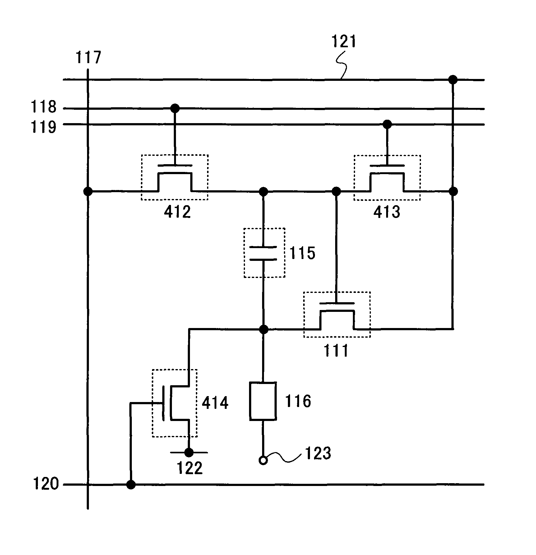
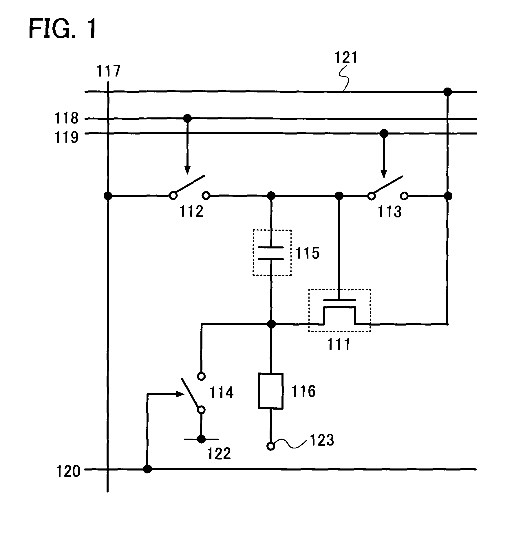
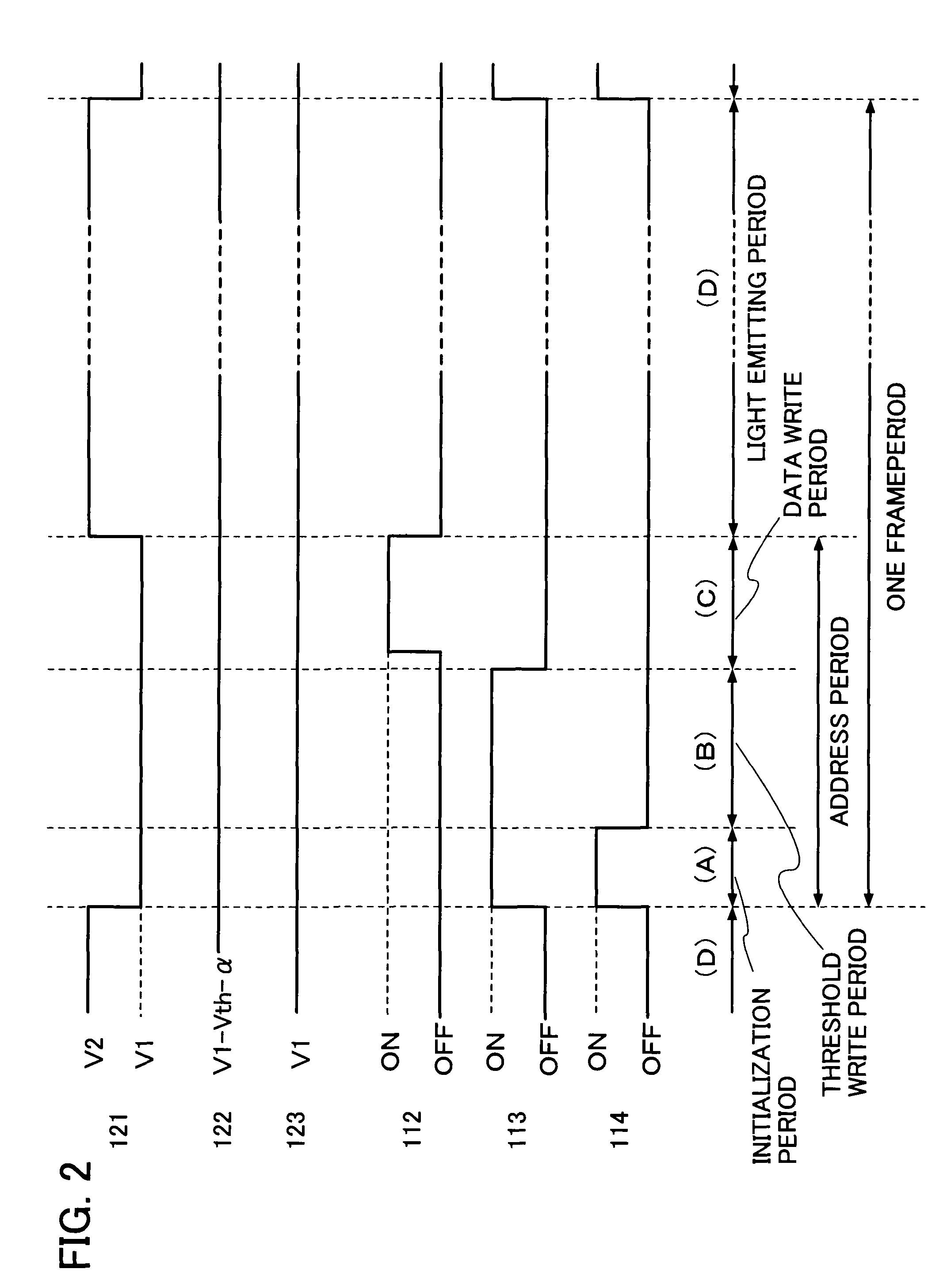
[0094]A basic structure of a pixel of the present invention is explained with reference to FIG. 1. The pixel shown in FIG. 1 includes a transistor 111, a first switch 112, a second switch 113, a third switch 114, a capacitor 115, and a light emitting element 116. Note that the pixel is connected to a signal line 117, a first scan line 118, a second scan line 119, a third scan line 120, a power supply line 121, and a potential supply line 122. In this embodiment mode, the transistor 111 is an n-channel transistor and is turned on when a gate-source voltage (Vgs) thereof exceeds a threshold voltage (Vth). In addition, a pixel electrode of the light emitting element 116 is an anode and an opposite electrode 123 is a cathode. Note that the gate-source voltage of the transistor is referred to as Vgs; a drain-source voltage, Vds; a threshold voltage, Vth; a voltage accumulated in the capacitor, Vcs; and the power supply line 121, the potential supply line 122, and the signal line 117 are ...

embodiment mode 2

[0144]In this embodiment mode, a pixel with a structure different from Embodiment Mode 1 is explained with reference to FIGS. 39A and 39B. Note that a common reference numeral is used to denote a component similar to Embodiment Mode 1, and detailed explanation of the same portion or a portion having a similar function is omitted.

[0145]The pixel shown in FIG. 39A includes a transistor 111, a first switch 112, a second switch 113, a rectifier element 3914, a capacitor 115, and a light emitting element 116. Note that the pixel is connected to a signal line 117, a first scan line 118, a second scan line 119, a third scan line 3920, and a power supply line 121. The pixel shown in FIG. 39A has a structure in which the rectifier element 3914 is used as the third switch 114 in FIG. 1, and a second electrode of the capacitor 115, a first electrode of the transistor 111, and a pixel electrode of the light emitting element 116 are connected to the third scan line 3920 through the rectifier ele...

embodiment mode 3

[0151]In this embodiment mode, pixels having structures different from those in Embodiment Mode 1 are explained with reference to FIGS. 7 to 9. Note that a common reference numeral is used to denote a component similar to Embodiment Mode 1, and detailed explanation of the same portion or a portion having a similar function is omitted.

[0152]A pixel 700 shown in FIG. 7 includes a transistor 111, a first switch 112, a second switch 113, a third switch 114, a capacitor 115, and a light emitting element 116. Note that the pixel 700 is connected to a signal line 117, a first scan line 718, a second scan line 119, a third scan line 120, a power supply line 121, and a first pixel line 718 of a subsequent row.

[0153]In the pixel of FIG. 1 described in Embodiment Mode 1, the first electrode of the transistor 111 is connected to the potential supply line 122 through the third switch 114, while it can be connected to the first scan line 718 of the subsequent row in FIG. 7. This is because the po...


PUM


Abstract

A load, a transistor which controls a current value supplied to the load, a capacitor, a power supply line, and first to third switches are provided. After a threshold voltage of the transistor is held by the capacitor, a potential in accordance with a video signal is inputted and a voltage that is the sum of the threshold voltage and the potential is held. Accordingly, variation in current value caused by variation in threshold voltage of the transistor can be suppressed. Therefore, a desired current can be supplied to a load such as a light emitting element. In addition, a display device with a high duty ratio can be provided by changing a potential of the power supply line.

Description

BACKGROUND OF THE INVENTION[0001]1. Field of the Invention[0002]The present invention relates to a semiconductor device functioning to control a current supplied to a load by a transistor, and a display device including a pixel formed using a current-drive display element of which luminance changes in accordance with a signal, and a signal line driver circuit and a scan line driver circuit which drive the pixel. The present invention also relates to a driving method thereof. Further, the present invention relates to an electronic device having the display device in a display portion.[0003]2. Description of the Related Art[0004]In recent years, a self-luminous display device using a light emitting element such as an electroluminescent (EL) element in a pixel, a so-called light emitting device has attracted attention. As a light emitting element used for such a self-luminous display device, an organic light emitting diode (OLED) and an EL element have attracted attention, and have bee...

Claims


Application Information

Patent Timeline
Patent Type & Authority Patents(United States)
IPC IPC(8): G09G3/30G09G3/36G09G5/00G06F3/038H05B44/00
CPCG09G3/3233H01L27/15G09G3/2022G09G2300/0819G09G2300/0842G09G2300/0861G09G2300/0866G09G2310/0256G09G2320/02G09G2320/0219G09G2320/0261G09G2320/043H01L27/3244G09G2310/0251H10K59/12G09G3/30G09G3/32G09G3/20H05B33/12H10K59/131G09G2320/0233H01L27/1255H01L29/78669H01L29/78678
Inventor KIMURA, HAJIME
Owner SEMICON ENERGY LAB CO LTD
Why Eureka
Try Eureka