
Wired circuit board and connection structure between wired circuit boards

a wired circuit board and connection structure technology, applied in the direction of printed circuit structure associations, printed circuit aspects, printed circuit manufacturing, etc., can solve the problems of difficult positioning, difficult to arrange the first connection terminal and the second connection terminal in line, etc., to prevent a relative displacement therebetween, accurate position of the first wired circuit board, and improve reliability

Inactive Publication Date: 2012-11-20
NITTO DENKO CORP
View PDF15 Cites 5 Cited by
  • Summary
  • Abstract
  • Description
  • Claims
  • Application Information

AI Technical Summary

Benefits of technology

[0010]It is therefore an object of the present invention to provide a wired circuit board and a connection structure between wired circuit boards which can ensure precise positioning of a first wired circuit board and a second wired circuit board and improve reliability.
[0023]In the connection structure between the wired circuit boards, the first opposed surface of the first wired circuit board and the second opposed surface of the second wired circuit board comprise the at least two types of interfitting surfaces extending in different directions. Therefore, by mutually interfitting the interfitting surfaces of the first opposed surface with the interfitting surfaces of the second opposed surface, it is possible to accurately position the first wired circuit board and the second wired circuit board and prevent a relative displacement therebetween. This can ensure accurate positioning of the first wired circuit board and the second wired circuit board and improve reliability.

Problems solved by technology

As a result, it becomes difficult to arrange the first connection terminal and the second connection terminal in line.
When a particular consideration is given to a recent conductive pattern which has a higher density and an increased number of wires, precise positioning of the first connecting terminal and the second connecting terminal is necessary, but such positioning becomes more difficult.

Method used


Image

  • Wired circuit board and connection structure between wired circuit boards
  • Wired circuit board and connection structure between wired circuit boards
  • Wired circuit board and connection structure between wired circuit boards

Examples


Embodiment Construction

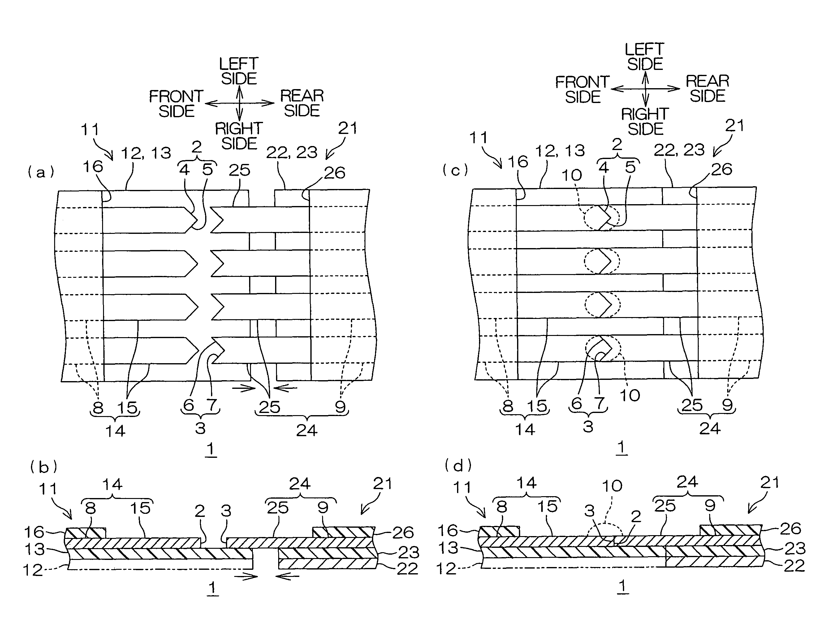
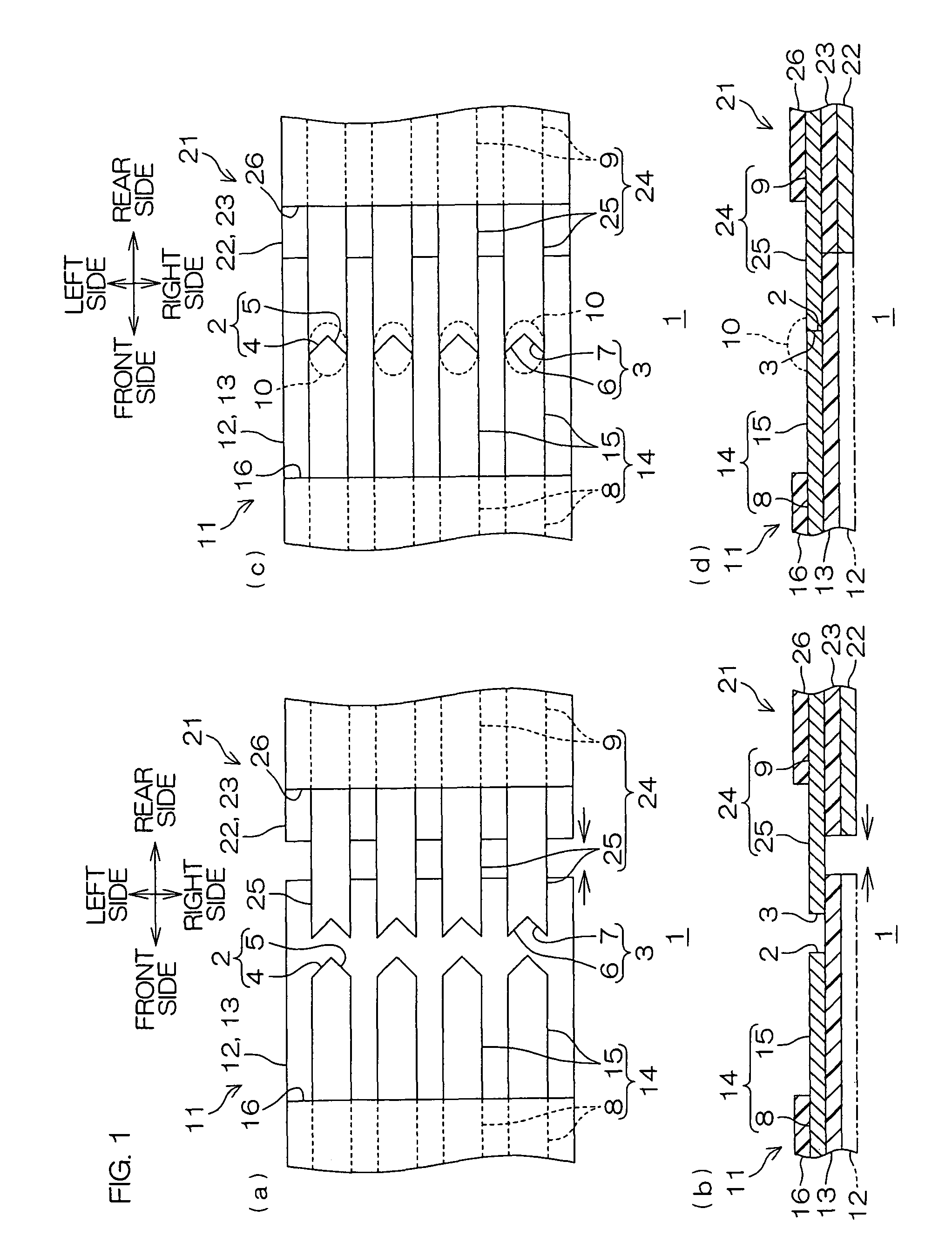
[0050]FIG. 1 shows a wired circuit board and a connection structure between wired circuit boards according to an embodiment of the present invention, (a) showing a plan view of the wired circuit boards before connection, (b) showing a cross-sectional view of FIG. 1(a) along a front-to-rear direction, (c) showing a plan view of the wired circuit board after connection, and (d) showing a cross-sectional view of FIG. 1(c) along the front-to-rear direction.

[0051]In FIGS. 1(a) and 1(c), the left side is defined as “front side”, the right side is “rear side”, the upper side is “left side”, and the lower side is “right side”.

[0052]In FIG. 1, the wired circuit board 1 includes a first wired circuit board 11 and a second wired circuit board 21. The first wired circuit board 11 and the second wired circuit board 21 are disposed to be opposed to each other in a front-to-rear direction such that the rear end portion of the first wired circuit board 11 is abutted against the front end portion of...


PUM


Abstract

A wired circuit board includes a first wired circuit board and a second wired circuit board disposed to be opposed to the first wired circuit board in the same plane. A first opposed surface of the first wired circuit board facing the second wired circuit board and a second opposed surface of the second wired circuit board facing the first wired circuit board include at least two types of interfitting surfaces extending in different directions so as to mutually interfit the first opposed surface with the second opposed surface.

Description

CROSS REFERENCE TO RELATED APPLICATION[0001]This application claims the benefit of U.S. Provisional Application No. 60 / 960,581, filed Oct. 4, 2007, and claims priority from Japanese Patent Application No. 2007-189942, filed Jul. 20, 2007, the contents of which are herein incorporated by reference in their entirety.BACKGROUND OF THE INVENTION[0002]1. Field of the Invention[0003]The present invention relates to a wired circuit board and to a connection structure between wired circuit boards. More particularly, the present invention relates to a wired circuit board in which two wired circuit boards are connected and to a connection structure therebetween.[0004]2. Description of the Related Art[0005]Conventionally, various connection structures between wired circuit boards have been proposed to connect two wired circuit boards.[0006]For example, a connection structure between wired circuit boards as shown below is proposed for visual inspection of electrical connections between the firs...

Claims


Application Information

Patent Timeline
Patent Type & Authority Patents(United States)
IPC IPC(8): H05K1/03H05K1/11H05K1/14
CPCH05K1/142H05K3/363H05K1/056H05K1/117H05K2201/058H05K2201/09145H05K2201/09381H05K2203/167
Inventor ISHII, JUNOOYABU, YASUNARITANAKA, TAKESHINAITO, TOSHIKI
Owner NITTO DENKO CORP
Learn More