Automatic debug apparatus and method for automatic debug of an integrated circuit design

a technology of automatic debugging and integrated circuits, applied in the direction of cad circuit design, program control, instruments, etc., can solve the problems of large amount of stimulation required to achieve significant test coverage of complex ics, large amount of failure data generated by continuous running stimulations, and large amount of time and mental effort of technicians to analyz

Active Publication Date: 2012-10-30
CADENCE DESIGN SYST INC
View PDF3 Cites 13 Cited by
  • Summary
  • Abstract
  • Description
  • Claims
  • Application Information

AI Technical Summary

Problems solved by technology

The complexity of modern designs for complex ICs typically requires large amounts of stimulation to achieve significant test coverage of design verification (e.g., to exercise the DUV sufficiently to demonstrate that the DUV works as desired).
The failures typically indicate potential problems with the DUV or the VE.
The output of failure information forms an important part of the verification process as the failure information may reveal design errors of the DUV and / or the VE that need to be debugged and fixed before an IC is fabricated.
Debugging a DUV is typically a challenging intellectual process that traditionally has been conducted by expert engineers.
Continuously running stimulations generates a relatively large amount of failure data to be reviewed for DUV debug by a team of design verification experts, technicians, and the like devoted to debugging.
Due to the relatively large amount of data generated by running a stimulation of a DUV these engineers and technicians spend relatively larges amount of time and mental effort to analyze data to locate bugs.
The debug process is a bottleneck in the design process, which affects engineering costs and schedules for moving IC to market.

Method used


Image

  • Automatic debug apparatus and method for automatic debug of an integrated circuit design
  • Automatic debug apparatus and method for automatic debug of an integrated circuit design
  • Automatic debug apparatus and method for automatic debug of an integrated circuit design

Examples


Embodiment Construction

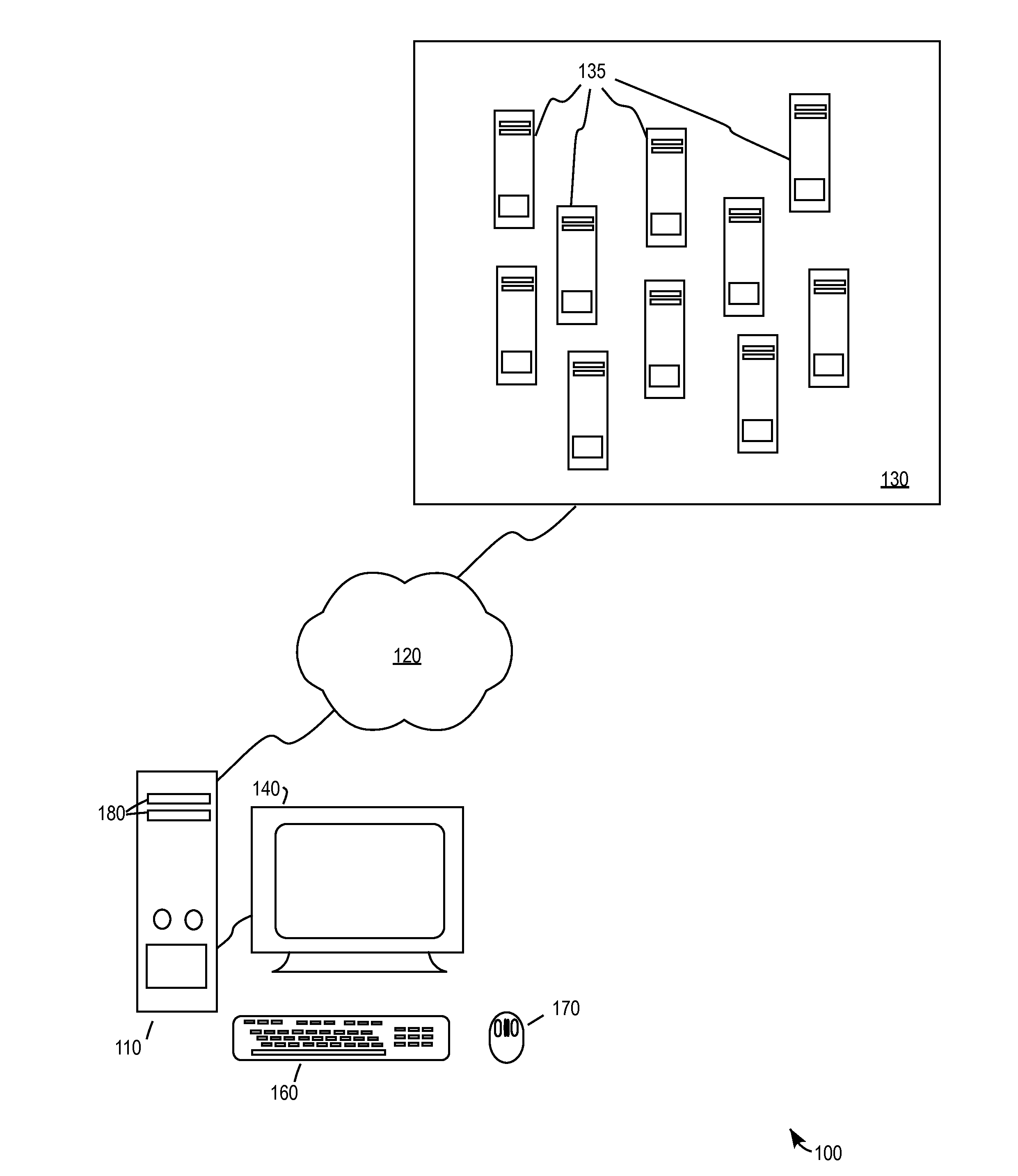
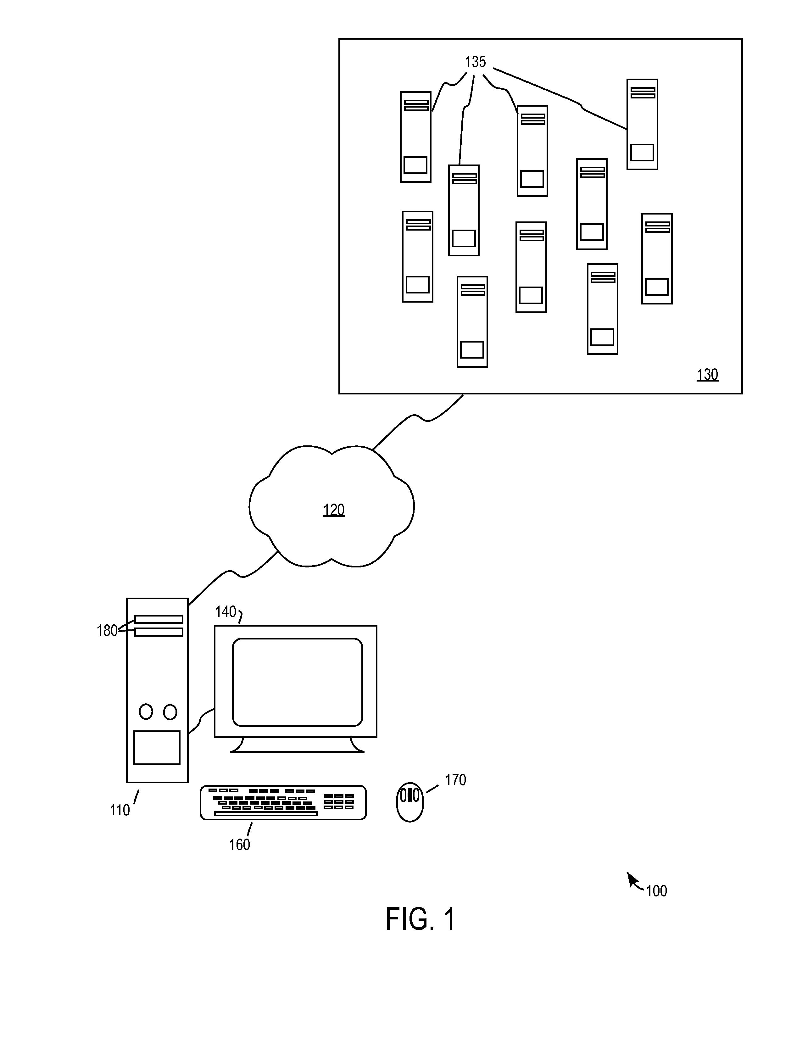
[0024]FIG. 1 is a simplified schematic of a computing system 100 according to one embodiment of the present invention. The computing system includes a user computer 110 coupled through a network 120 to a computer farm 130. The user computer may be a personal computer (such as a desktop computer), a work station, a laptop computer, or the like. The user computer may be a computer at which a circuit designer, a computer programmer, a debug engineer, or the like may work to generate a design for an integrated circuit, write a computer program to verify the design, and debug the design based on failure data generated by a verification program (sometimes referred to herein as a verification environment). The user computer may include a computer monitor 140 on which audiovisual data may be presented to a user (e.g., a human user). The user computer may also include one or more control devices, such as a keyboard 160, a mouse 170, a puck, a joystick, etc. The user computer may also include...


PUM


Abstract

A computerized method of characterizing a DUV includes executing in a verification environment (VE) a set of verification tests to stimulate the DUV to collect test results from the DUV. The method further includes collecting a set of failure data for the test results; and generating sets of common failures based on clusters of features of interest in the set of failure data. The method further includes generating a set of hints from the common failures; wherein the hints indicate a potential failure mode or a potential root cause failure of the DUV for the test results for the simplified set of tests; and generating a set of debug data from the clusters of features of interest. The method further includes transferring the set of hints and the set of debug data to a user computer for storage, display, and use in an interactive debug session of the DUV.

Description

BACKGROUND OF THE INVENTION[0001]The present invention generally relates to an apparatus and a method for circuit design. More particularly, the present invention generally relates to an apparatus and method for automating the debug of design models and verification environments for integrated circuits.[0002]Modern circuit design of integrated circuits (ICs) is a combination of automated design and debug of the design. ICs are often automatically designed using specialized computer program code that serves as simulation of the IC. The design of complex ICs generally requires a high level of design verification before millions of dollars are committed to the manufacture of the ICs. Design verification typically includes running a verification program on a design (often referred to as a DUV, or design under verification). Much of the verification is carried out by stimulation of the DUV at a logical level, where the DUV is modeled with one or more hardware description languages (HDLs)...

Claims


Application Information

Patent Timeline
Patent Type & Authority Patents(United States)
IPC IPC(8): G06F9/455G06F17/50
CPCG01R31/31705G06F11/26G06F17/5022G06F30/33
Inventor HOLLANDER, YOAVFELDMAN, YAEL
Owner CADENCE DESIGN SYST INC
Why Eureka
Try Eureka