
Vertically-oriented semiconductor selection device providing high drive current in cross-point array memory

a semiconductor and cross-point array technology, applied in the direction of semiconductor devices, basic electric elements, electrical appliances, etc., can solve the problems of large space occupation and power consumption of non-volatile memory devices, cell shrinkage, and extremely high current densities

Active Publication Date: 2012-09-25
MICRON TECH INC
View PDF18 Cites 46 Cited by
  • Summary
  • Abstract
  • Description
  • Claims
  • Application Information

AI Technical Summary

Problems solved by technology

Traditionally, non-volatile memory devices occupied large amounts of space and consumed large quantities of power.
However, these high currents result in extremely high current densities as the size of the memory cells continues to shrink.

Method used


Image

  • Vertically-oriented semiconductor selection device providing high drive current in cross-point array memory
  • Vertically-oriented semiconductor selection device providing high drive current in cross-point array memory
  • Vertically-oriented semiconductor selection device providing high drive current in cross-point array memory

Examples


Embodiment Construction

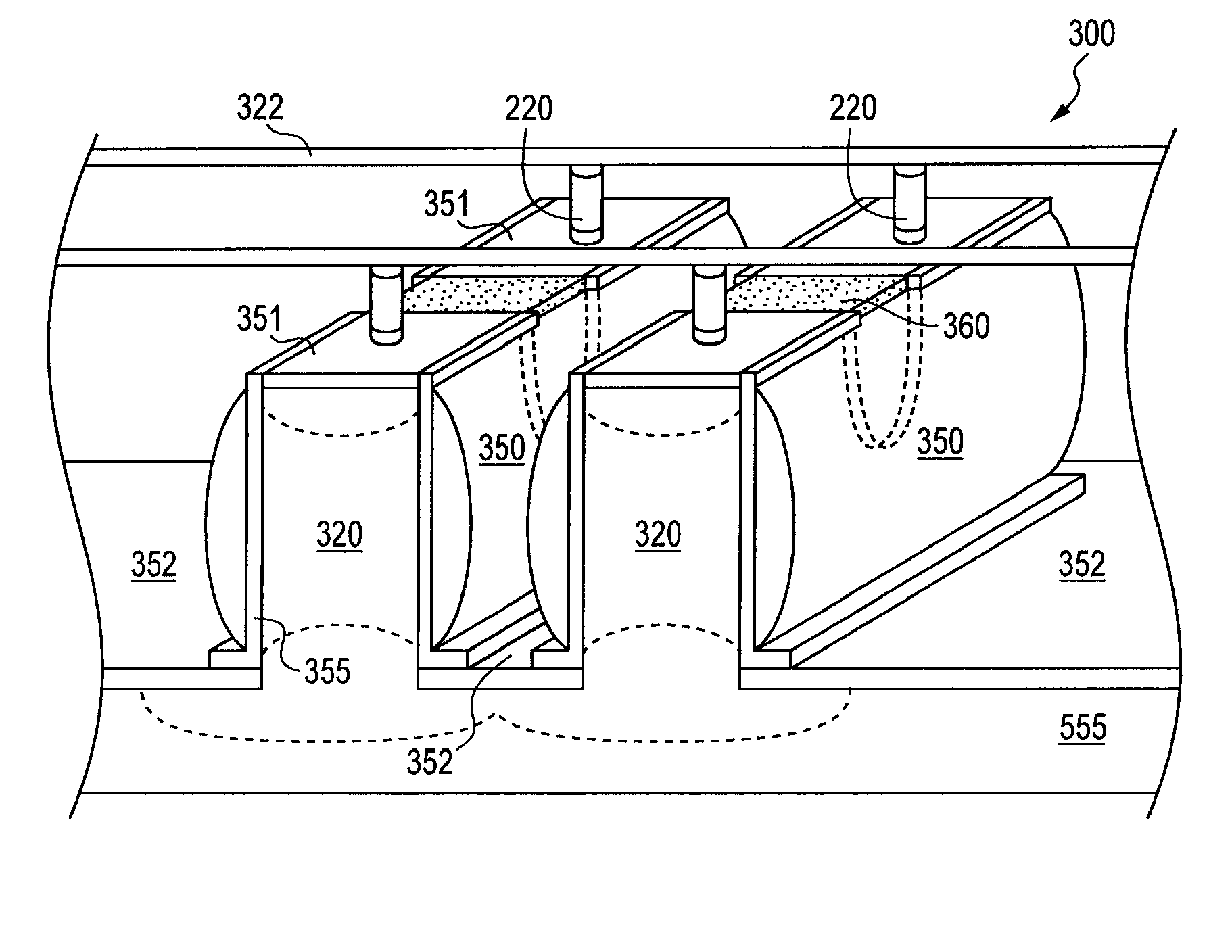
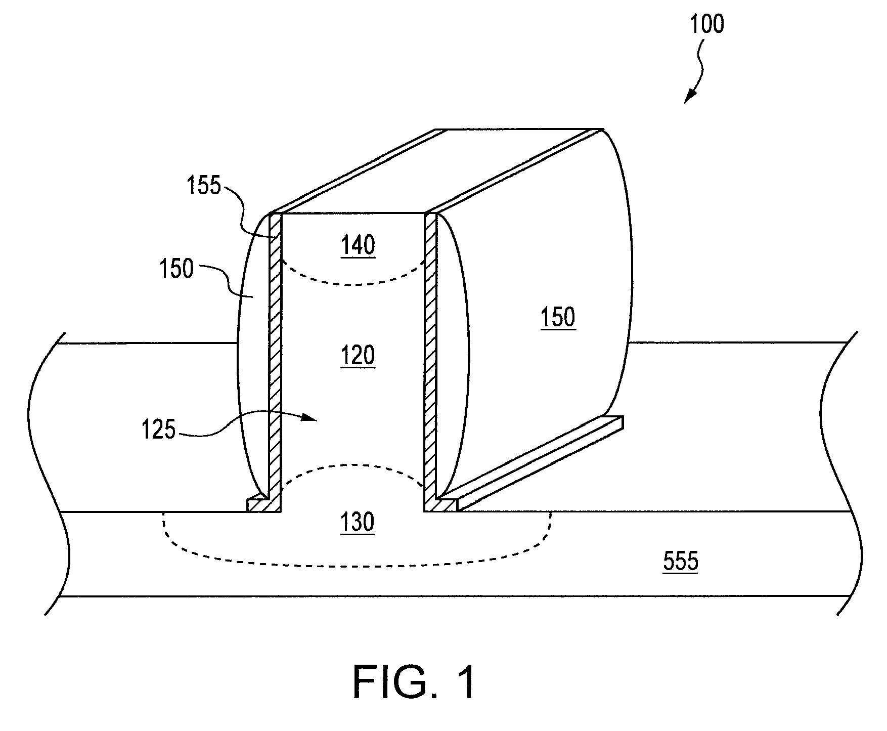
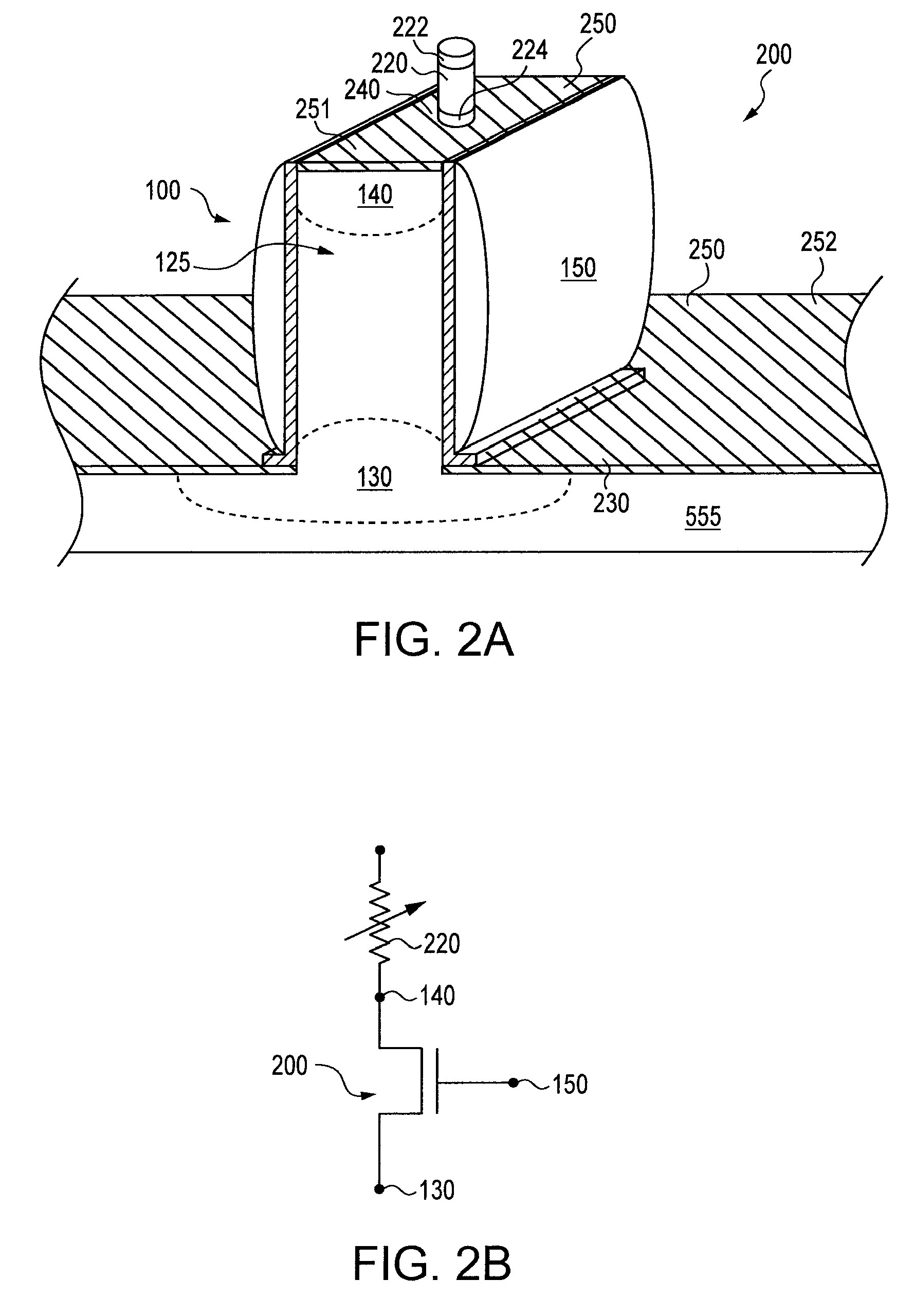
[0012]Traditional memory access devices are planar in nature, meaning that the access devices are formed layer by layer within the plane of the underlying structure. The underlying structure includes a substrate that is a base material and layers formed on the surface of the substrate. The substrate and overlaying layers on top of the substrate are flat or planar. The access devices are formed within these layers so that the resulting devices are also laid out in a planar arrangement. As a specific example, a planar field-effect transistor (“FET”) is a FET with a conductive channel that is within the layers of the underlying structure. Planar access devices have a relatively large footprint and suffer from leakage currents or must be isolated from each other in order to avoid leakage currents.

[0013]Non-planar access devices are alternatives to planar devices. Non-planar access devices are access devices that are not flat or planar and can be oriented in a vertical direction from a s...


PUM


Abstract

A vertical semiconductor material mesa upstanding from a semiconductor base that forms a conductive channel between first and second doped regions. The first doped region is electrically coupled to one or more first silicide layers on the surface of the base. The second doped region is electrically coupled to one of a plurality of second silicide layers on the upper surface of the mesa. A gate conductor is provided on one or more sidewalls of the mesa.

Description

CROSS-REFERENCE TO RELATED APPLICATIONS[0001]This application is related to U.S. patent application Ser. No. 12 / 469,433, filed concurrently herewith, the specification of which is herein incorporated by reference in its entirety.FIELD OF THE INVENTION[0002]The embodiments disclosed herein relate generally to the field of semiconductor selection devices and, more particularly, to access devices for semiconductor memory devices.BACKGROUND OF THE INVENTION[0003]A non-volatile memory device is capable of retaining stored information even when power to the memory device is turned off. Traditionally, non-volatile memory devices occupied large amounts of space and consumed large quantities of power. As a result, non-volatile memory devices have been widely used in systems where limited power drain is tolerable and battery-life is not an issue. However, as systems requiring non-volatile memories have continued to shrink in size, improvements in non-volatile memory devices have been sought i...

Claims


Application Information

Patent Timeline
Patent Type & Authority Patents(United States)
IPC IPC(8): H01L29/66
CPCH01L27/2463H01L27/2454H01L29/7827H01L45/06H01L45/1233H10B63/34H10B63/80H10N70/231H10N70/826
Inventor SANDHU, GURTEJZAHURAK, JOHN K.PARKS, JAY
Owner MICRON TECH INC
Learn More