Substrate device with a transmission line connected to a connector pad and method of manufacture

a technology of connector pads and substrate devices, which is applied in the direction of contact member manufacturing, waveguides, high frequency circuit adaptations, etc., can solve the problems of reflection noise, impedance mismatch, and degradation of signal quality (signal waveform), so as to reduce the degradation of signal waveform, reduce the effect of refection noise and reducing the amount of capacitan

Inactive Publication Date: 2012-09-04
NEC CORP
View PDF11 Cites 0 Cited by
  • Summary
  • Abstract
  • Description
  • Claims
  • Application Information

AI Technical Summary

Benefits of technology

[0012]According to the present invention, the pad is formed such that the part of the pad on the transmission line side and part of the pad on the opposite side of the transmission line are electrically insulated from each other. Thus, it is possible to reduce refection noise from the stub end to reduce degradation of a signal waveform. Further, it is possible to reduce an unnecessary capacitance between the stub and ground layer to thereby improve impedance mismatch.

Problems solved by technology

Particularly, in high-speed signal transmission, this portion may be a source of noise, resulting in degradation of signal quality (signal waveform).
This may cause impedance mismatch, leading to reflection noise.
Particularly, in high-speed signal transmission, influence of the reflection noise becomes large relative to the noise margin of a signal in the voltage axis direction and time axis direction, making it difficult to secure the eye pattern in a signal waveform.

Method used


Image

  • Substrate device with a transmission line connected to a connector pad and method of manufacture
  • Substrate device with a transmission line connected to a connector pad and method of manufacture
  • Substrate device with a transmission line connected to a connector pad and method of manufacture

Examples


Embodiment Construction

[0021]An exemplary embodiment of a substrate device according to the present invention will be described in detail below with reference to the accompanying drawings. Through the following description, the same reference numerals as those in FIG. 8 denote the same or corresponding parts as those in FIG. 8.

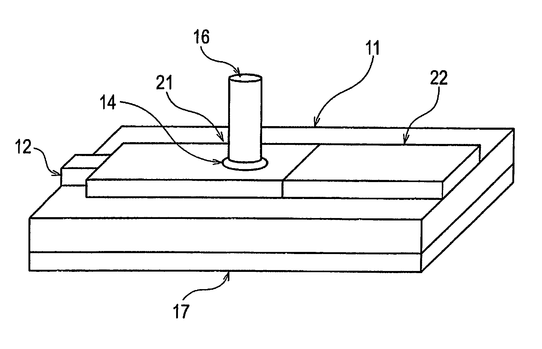
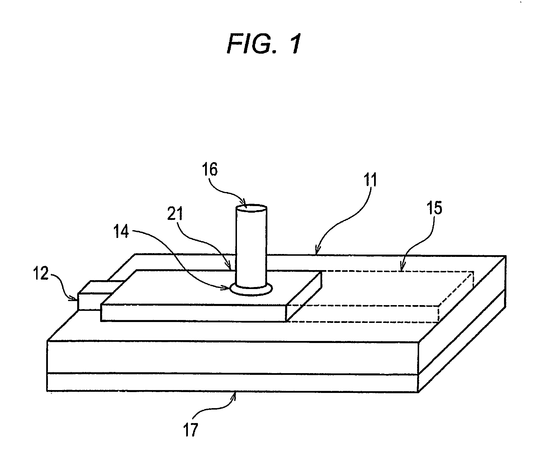
[0022]FIG. 1 is a substrate device according to an exemplary embodiment of the present invention. In the substrate device illustrated in FIG. 1, a transmission line 12 serving as a signal line is mounted on a printed board 11. The transmission line 12 is connected to a pad 21 for an edge connector 16 at the end of the board. The pad 21 and edge connector 16 are connected to each other at a contact point 14. A transmission signal is transmitted from the transmission line 12 to the edge connector 16 via the pad 21 and contact point 14, or transmitted in the reverse direction from the edge connector 16 to the transmission line 12 via the contact point 14 and pad 21.

[0023]As described a...


PUM

PropertyMeasurementUnit
electrically insulatingaaaaaaaaaa
connection structureaaaaaaaaaa
transmissionaaaaaaaaaa

Abstract

A substrate device includes: a substrate; a ground layer disposed on one of two opposing surfaces of the substrate; a transmission line disposed on the other of the two opposing surfaces of the substrate; a pad which is disposed on the other of the two opposing surfaces of the substrate and connected to the transmission line; and a connector connected to the pad via a contact point. The pad has a part on the transmission line side and a part positioned on the opposite side of the transmission line with respect to the contact point with the connector which are electrically insulated from each other.

Description

TECHNICAL FIELD[0001]The present invention relates to a substrate device and its manufacturing method and, more particularly, to a substrate device having a pad structure for an edge connector provided at the end of a printed board and a manufacturing method of such a substrate device.BACKGROUND ART[0002]A connection structure of a substrate device of the related art will be described with reference to FIG. 8.[0003]Referring to FIG. 8, a transmission line 12 serving as a signal line is mounted on a printed board 11. The transmission line 12 is connected to a pad 13 for an edge connector 16 at the end of the board. The pad 13 and edge connector 16 are connected to each other at a contact point 14. A transmission signal is transmitted from the transmission line 12 to the edge connector 16 via the pad 13 and contact point 14, or transmitted in the reverse direction from the edge connector 16 to the transmission line 12 via the contact point 14 and pad 13.[0004]The pad 13 for the edge c...

Claims


Application Information

Patent Timeline
Patent Type & Authority Patents(United States)
IPC IPC(8): H01P5/02
CPCH05K1/0216H05K1/024H05K1/025H05K1/117Y10T29/49204H05K2201/09663H05K2201/09909H05K2201/10318H05K2201/0792
Inventor OOTSUKA, HIDETAKA
Owner NEC CORP
Why Eureka
Try Eureka