Display apparatus and production method thereof
a technology of display apparatus and production method, which is applied in the manufacture of electrode systems, electric discharge tubes/lamps, discharge tubes luminescent screens, etc., can solve the problems of adverse effect, difficulty in obtaining the opening width of current technology, and further reducing the size of conventional pixels, so as to achieve the effect of reducing the pixel aperture ratio and improving the resolution feeling
- Summary
- Abstract
- Description
- Claims
- Application Information
AI Technical Summary
Benefits of technology
Problems solved by technology
Method used
Image
Examples
example 1
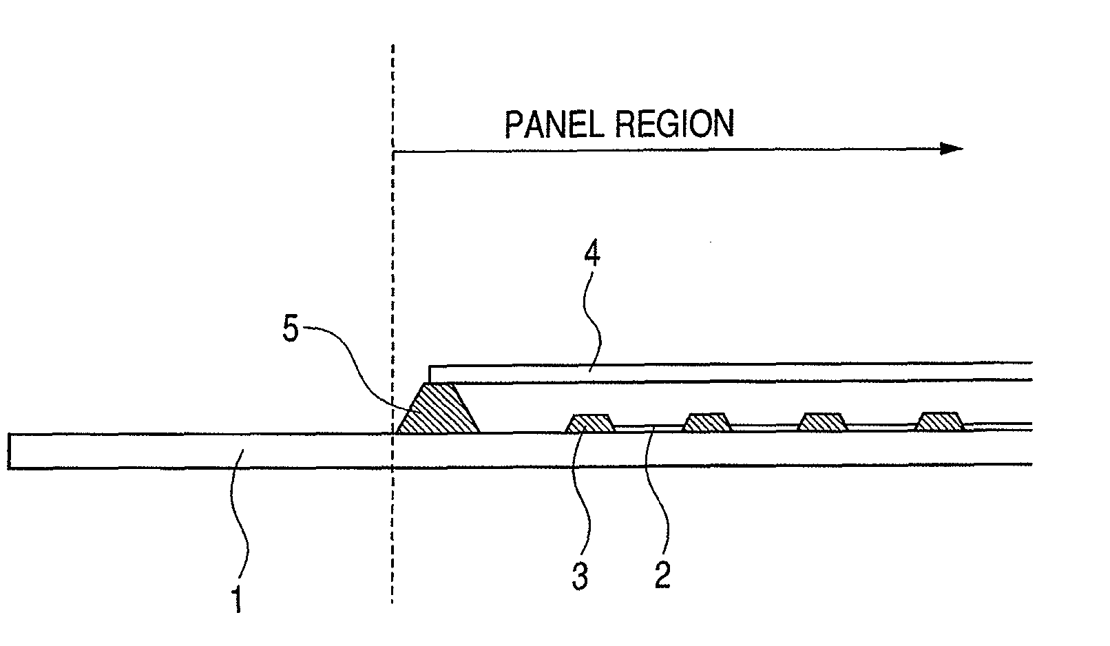
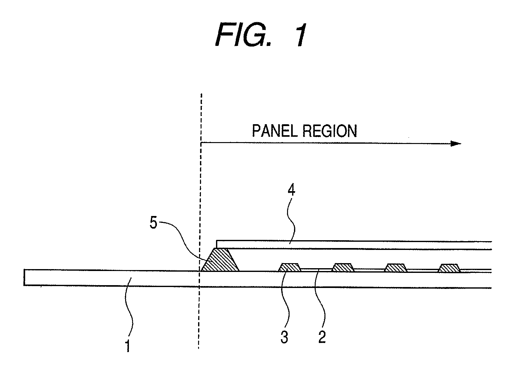
[0038]An organic EL display apparatus having a structure illustrated in FIG. 1 was produced.
[0039]Thin film transistors (TFTs), electrode wirings, and pixel electrodes, which are not shown, are formed in a matrix pattern on a substrate 1 illustrated in FIG. 1. One of glass, quartz, and a plastic film such as polyethylene terephthalate (PET), polycarbonate (PC), or polyethersulfone (PES) can be used for the substrate 1.
[0040]An organic compound for a light-emitting layer is formed on each of the pixel electrodes. An upper electrode is formed on the light-emitting layer. A protective film is formed on the upper electrode in some cases. In this example, the pixel electrodes, the organic compounds, and the upper electrodes, which are formed in a matrix pattern, compose a plurality of organic EL light-emitting portions (sub pixels) 2. The organic compounds for R, G, and B sub pixels are formed by evaporation to the organic EL light-emitting portions 2.
[0041]The respective organic EL ligh...
example 2
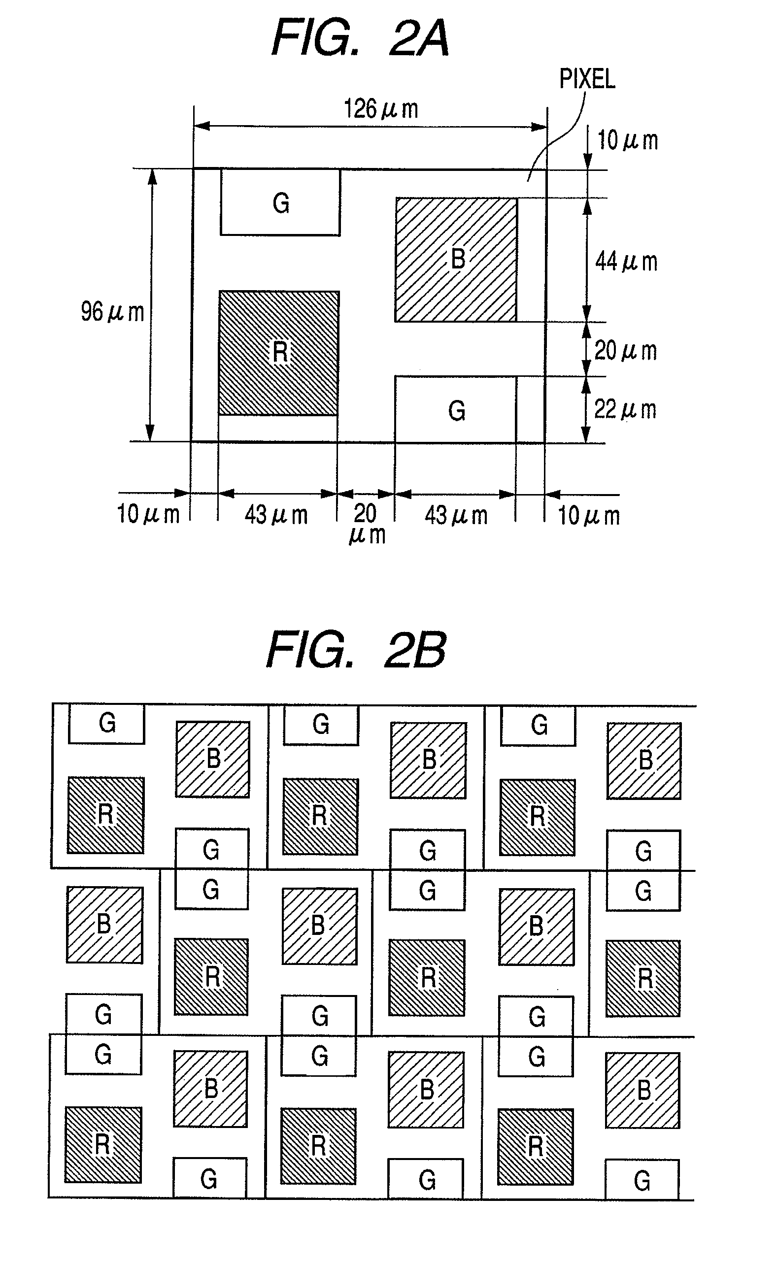
[0063]In order to confirm the superiority of the pixel and sub pixel disposition in the present invention, an image modeling a display panel having the pixel and sub pixel disposition in the present invention as illustrated in FIG. 6 was produced on a positive color film by exposure.
[0064]As illustrated in FIG. 6, the R sub pixel and the B sub pixel are disposed within each pixel in diagonal positions so as to partially overlap each other in any one of the two directions (vertical direction in this example) within the display surface. The two G sub pixels are disposed within each pixel in diagonal positions and distant from each other in the vertical direction.
[0065]With respect to other pixels adjacent to each other in the vertical direction, G sub pixels are adjacent to each other, an R sub pixel is adjacent to a B sub pixel, and a B sub pixel is adjacent to an R sub pixel. With respect to other pixels adjacent to each other in the other of the two directions within the display su...
example 3
[0090]In order to confirm the superiority of the pixel and sub pixel disposition in the present invention, an image modeling a display panel having the pixel and sub pixel dispositions in the present invention as illustrated in FIG. 9 was produced on a positive color film by exposure.
[0091]As illustrated in FIG. 9, with respect to the sub pixel disposition of pixels adjacent to each other in the vertical direction, line symmetry about a boundary line between the adjacent pixels as a symmetry axis is employed. In other words, the pixels adjacent to each other in the vertical direction have sub pixel dispositions reverse to each other in the vertical direction. With respect to the pixel disposition, the pixels adjacent to each other in the vertical direction are disposed in a grid pattern without offset of a pixel pitch in the horizontal direction.
[0092]In this example, the pixels adjacent to each other in the vertical direction are disposed in the grid pattern without offset of the p...
PUM
 Abstract
Description
Claims
Application Information
 - R&D
- Intellectual Property
- Life Sciences
- Materials
- Tech Scout
- Unparalleled Data Quality
- Higher Quality Content
- 60% Fewer Hallucinations
Browse by: Latest US Patents, China's latest patents, Technical Efficacy Thesaurus, Application Domain, Technology Topic, Popular Technical Reports.
© 2025 PatSnap. All rights reserved.Legal|Privacy policy|Modern Slavery Act Transparency Statement|Sitemap|About US| Contact US: help@patsnap.com


