Texture process and structure for manufacture of composite photovoltaic device substrates
a technology of photovoltaic device and substrate, applied in the field of solar energy techniques, can solve the problems of increasing oil consumption, solar cells still have limitations, and oil is becoming scarce, and achieves the effects of reducing material costs, reducing production costs, and reducing production costs
- Summary
- Abstract
- Description
- Claims
- Application Information
AI Technical Summary
Benefits of technology
Problems solved by technology
Method used
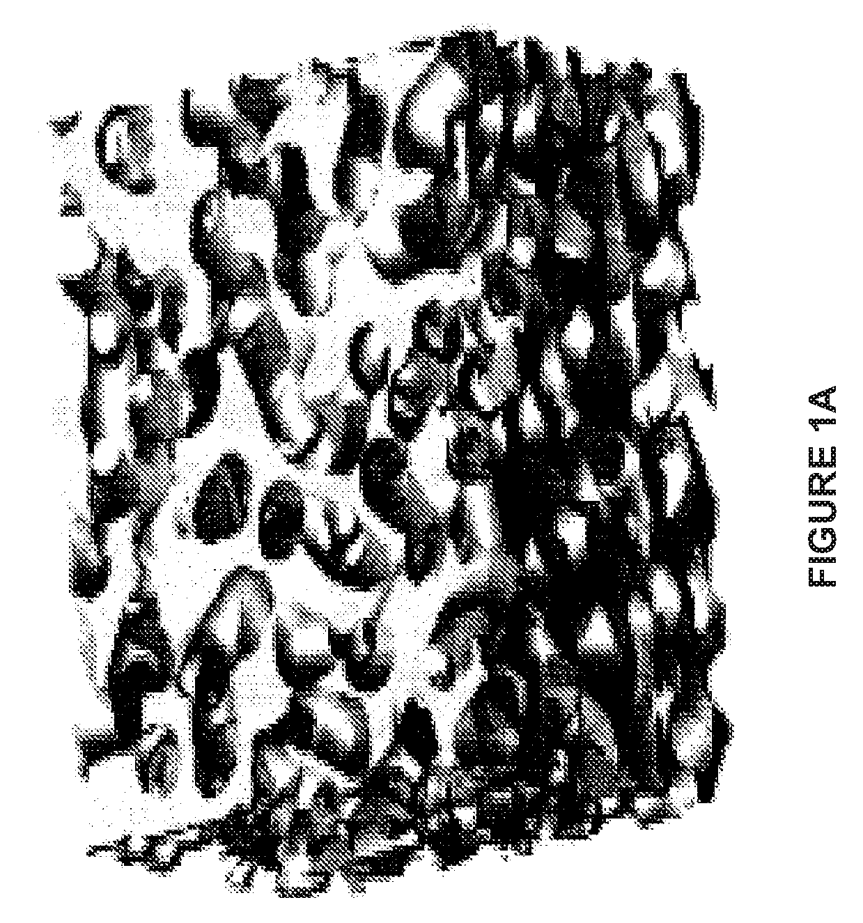
Image


Examples
Embodiment Construction
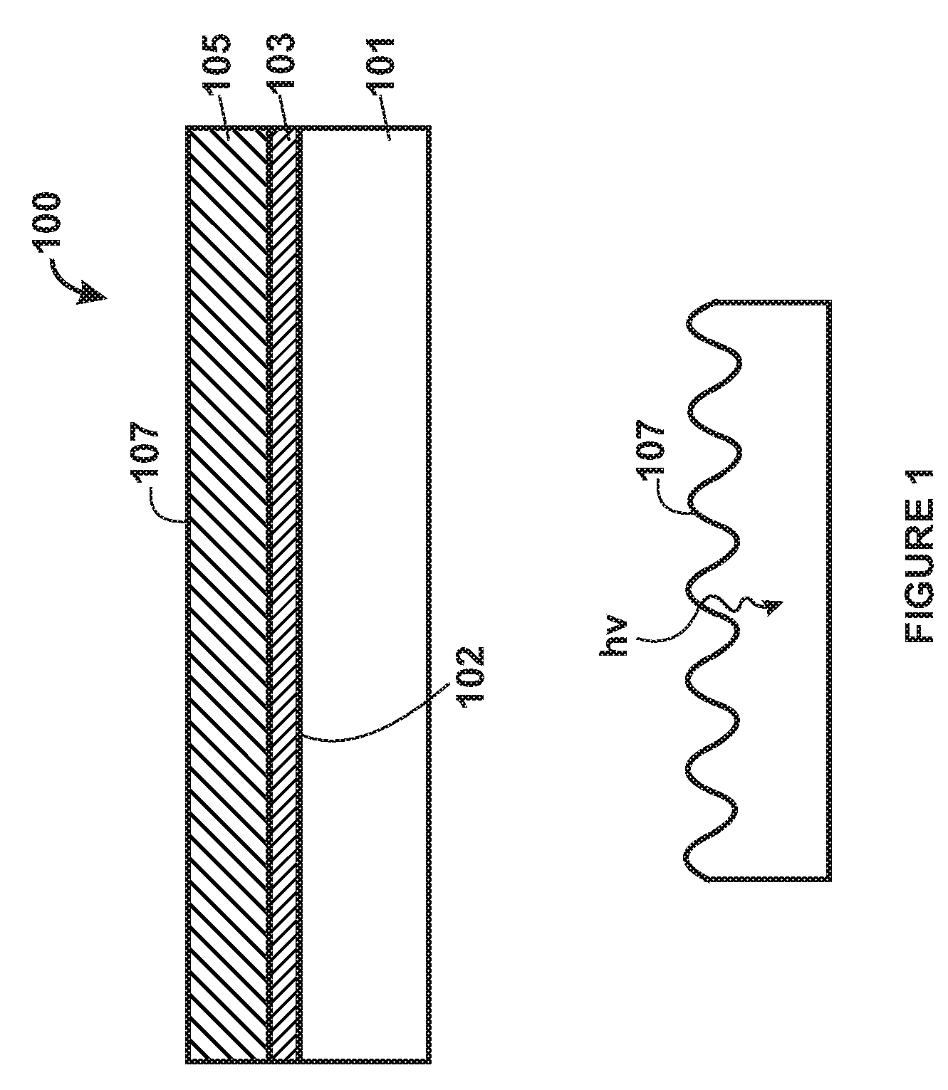
[0029]According to the present invention, techniques related to solar energy are provided. In particular, the present invention provides a method and resulting device fabricated for solar cell structures with high efficiency and low material costs. More particularly, the present invention provides a method and resulting device for manufacturing solar cells with thin photovoltaic regions provided on a fabric. Merely by way of example, the invention has been applied to solar cells and solar panels, commonly termed modules, but it would be recognized that the invention has a much broader range of applicability.
[0030]FIG. 1 is a simplified side-view diagram of a photovoltaic device according to an embodiment of the present invention. This diagram is merely an example, which should not unduly limit the scope of the claims herein. One of ordinary skill in the art would recognize many variations, modifications, and alternatives. As shown is a based material for a photovoltaic device 100. T...
PUM
| Property | Measurement | Unit |
|---|---|---|
| surface roughness | aaaaa | aaaaa |
| surface roughness | aaaaa | aaaaa |
| size | aaaaa | aaaaa |
Abstract
Description
Claims
Application Information
 - R&D
- Intellectual Property
- Life Sciences
- Materials
- Tech Scout
- Unparalleled Data Quality
- Higher Quality Content
- 60% Fewer Hallucinations
Browse by: Latest US Patents, China's latest patents, Technical Efficacy Thesaurus, Application Domain, Technology Topic, Popular Technical Reports.
© 2025 PatSnap. All rights reserved.Legal|Privacy policy|Modern Slavery Act Transparency Statement|Sitemap|About US| Contact US: help@patsnap.com