
Electrical connector soldered on a printed circuit board

a technology of printed circuit board and soldering portion, which is applied in the direction of fixed connections, coupling device connections, and coupling protection earth/shielding arrangements, etc., can solve the problems of affecting the use life of usb connectors, printed circuit boards, and affecting the electrical connection of soldering portions. , to achieve the effect of prolonging the life of electrical connectors

Inactive Publication Date: 2012-03-27
CHENG UEI PRECISION IND CO LTD
View PDF7 Cites 18 Cited by
  • Summary
  • Abstract
  • Description
  • Claims
  • Application Information

AI Technical Summary

Benefits of technology

[0008]As described above, the second soldering portion are vertically soldered on the second soldering points of the printed circuit board to make the electrical connector mounted to the printed circuit board, so when the mated connector is inserted into the inserting space of the shielding shell, the interacting force between copper foils which is covered on the printed circuit board and the printed circuit board will be decreased, then the possibility of the copper foils falling off from the printed circuit board will be greatly decreased. Therefore, a steady electrical connection between the electrical connector and the printed circuit board is realized, the life of the electrical connector is lengthened.

Problems solved by technology

On the other hand, if the user makes a mistake of moving away the USB connector, the soldering portion will afford a larger upward pulling force, it will be apt to make the copper foil which is covered on the soldering contact be torn open, so that a bad influence will be brought to the electrical connection of the soldering portion and the printed circuit board.
Therefore, the USB connector may work abnormally, the using life of the USB connector may also be affected.

Method used


Image

  • Electrical connector soldered on a printed circuit board
  • Electrical connector soldered on a printed circuit board
  • Electrical connector soldered on a printed circuit board

Examples


Embodiment Construction

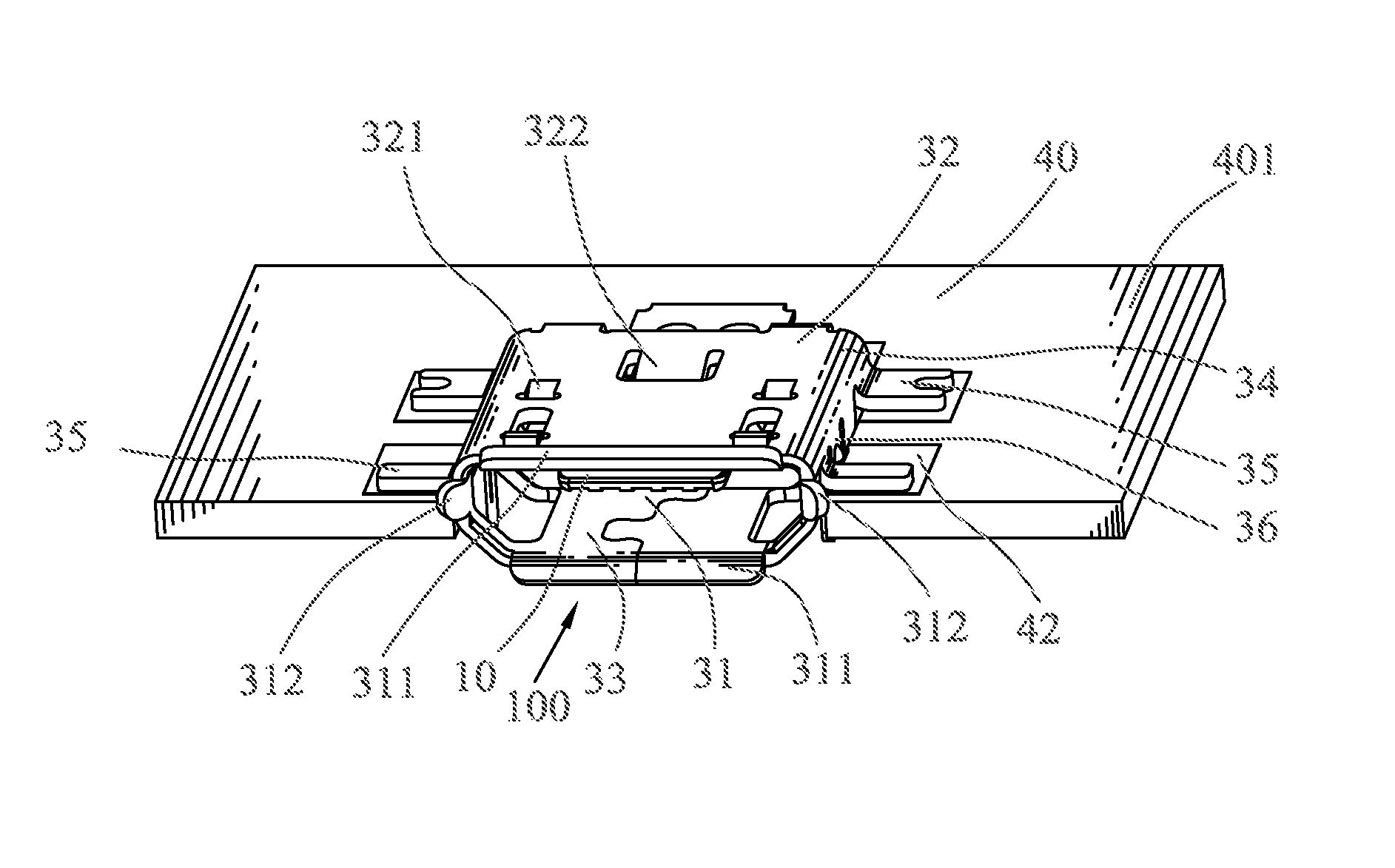
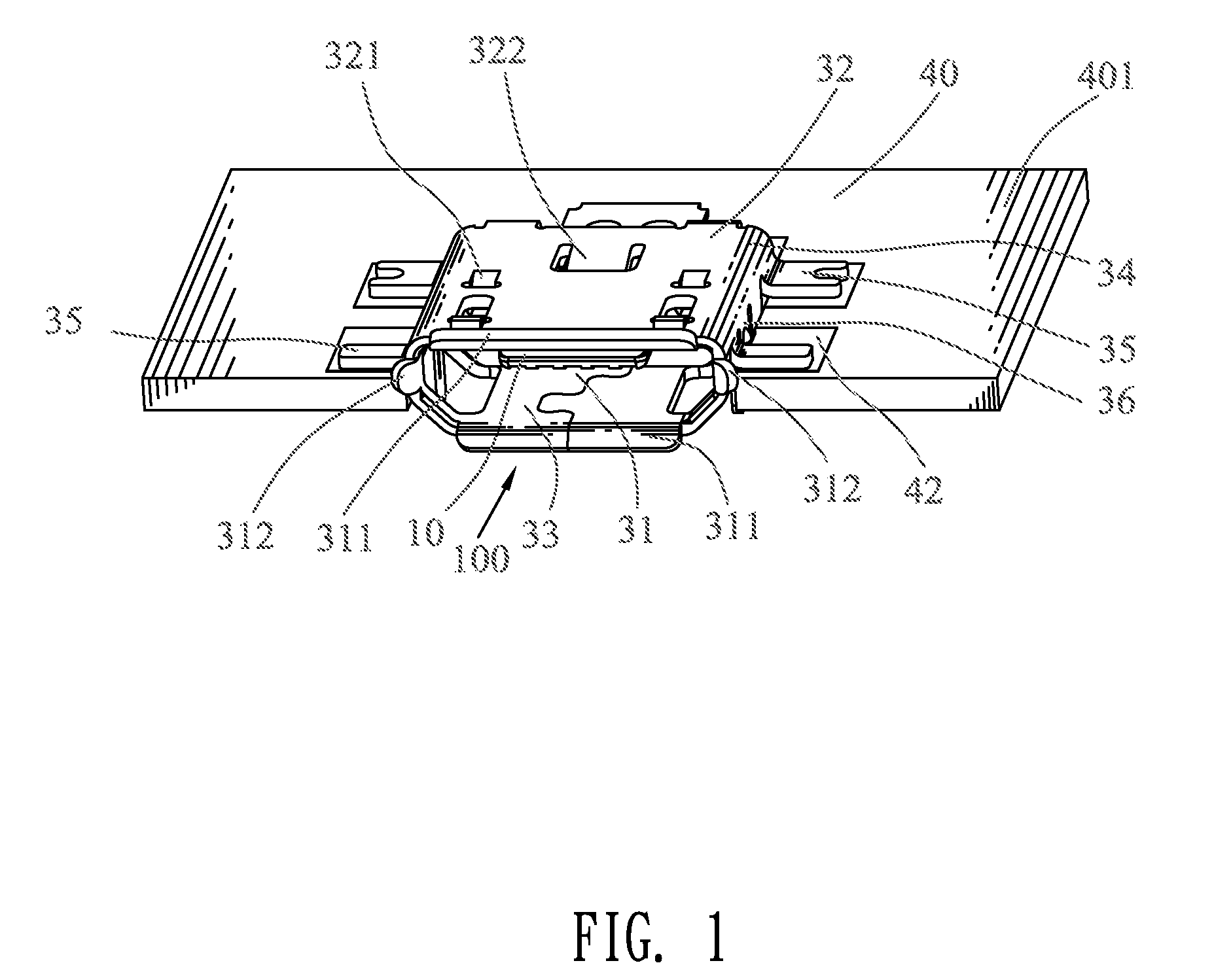
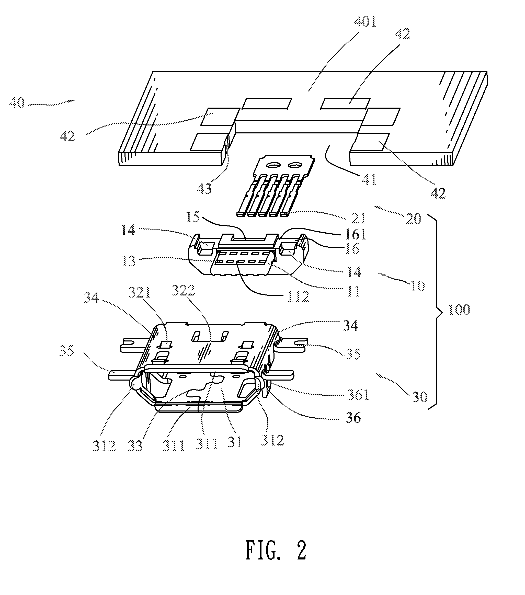
[0013]Referring to FIG. 2, an electrical connector 100 in accordance with the present invention is used to be soldered to a printed circuit board 40. The electrical connector 100 includes an insulating housing 10, a plurality of conductive terminals 20 received in the insulating housing 10, a shielding shell 30 enclosing the insulating housing 10.

[0014]Referring to FIG. 2-FIG. 3, the insulating housing 10 includes a base portion 16 and a tongue board 11 extended frontward from a front of the base portion 16. A bottom surface 111 of the tongue board 11 defines a plurality of fillisters 12 extending along a front-to-rear direction. A front and a rear of a top surface 112 of the tongue board 11 define two parallel rows of through-holes 13 vertically penetrating therethrough, respectively. Each two longitudinally arranged through-holes 13 are communicated with the corresponding fillisters 12. Two sides of a top surface 161 of the base portion 16 define two clipping grooves 14 passing th...


PUM


Abstract

An electrical connector is soldered on a printed circuit board. The printed circuit board has a containing gap opened at one side thereof. A top surface of the printed circuit board defines a plurality of first soldering points arranged around the containing gap. Each of two opposite inner sidewalls of the containing gap defines a second soldering point. The electrical connector is located in the containing gap. The electrical connector includes an insulating housing, a plurality of terminals and a shielding shell. The terminals are received in the insulating housing. The shielding shell defines an inserting space enclosing the insulating housing and the terminals. Each side plate has a first soldering portion extended outward and a second soldering portion extended downward therefrom. The second soldering portions are soldered on the second soldering points. The first soldering portions are soldered on the corresponding first soldering points.

Description

BACKGROUND OF THE INVENTION[0001]1. Field of the Invention[0002]The present invention generally relates to an electrical connector, and more particularly to an electrical connector which has a shielding shell capable of being soldered to a printed circuit board firmly.[0003]2. The Related Art[0004]With the development of electronic products, connections between a variety of electronic products and peripheral products thereof are more and more popular. The electronic product and the peripheral product thereof are usually connected by a USB connector. So, using frequencies of the USB connector are increased. The USB connector is widely used in the electronic products, the quality of the USB connector is requested higher and higher. In order to meet the quality request of the customers, the manufacturers have to make it firmly connect with a mated connector.[0005]A conventional USB connector includes an insulating housing, a plurality of terminals and a shielding shell. The insulating ...

Claims


Application Information

Patent Timeline
Patent Type & Authority Patents(United States)
IPC IPC(8): H01R13/648
CPCH01R12/725H01R12/57
Inventor YU, SHENG-NAN
Owner CHENG UEI PRECISION IND CO LTD
Learn More