Radiation-emitting semiconductor body with carrier substrate and method for the producing the same

Inactive Publication Date: 2012-01-03
OSRAM OPTO SEMICON GMBH & CO OHG
View PDF23 Cites 0 Cited by
  • Summary
  • Abstract
  • Description
  • Claims
  • Application Information

AI Technical Summary

Benefits of technology

[0007]One object of the present invention is to specify a simplified and cost-effective method for producing radiation-emitting semiconductor bodies with a carrier substrate. A further object of the present invention is to sp

Problems solved by technology

Semiconductor bodies such as these cannot be prod

Method used


Image

  • Radiation-emitting semiconductor body with carrier substrate and method for the producing the same
  • Radiation-emitting semiconductor body with carrier substrate and method for the producing the same
  • Radiation-emitting semiconductor body with carrier substrate and method for the producing the same

Examples


Example

DETAILED DESCRIPTION OF THE DRAWINGS

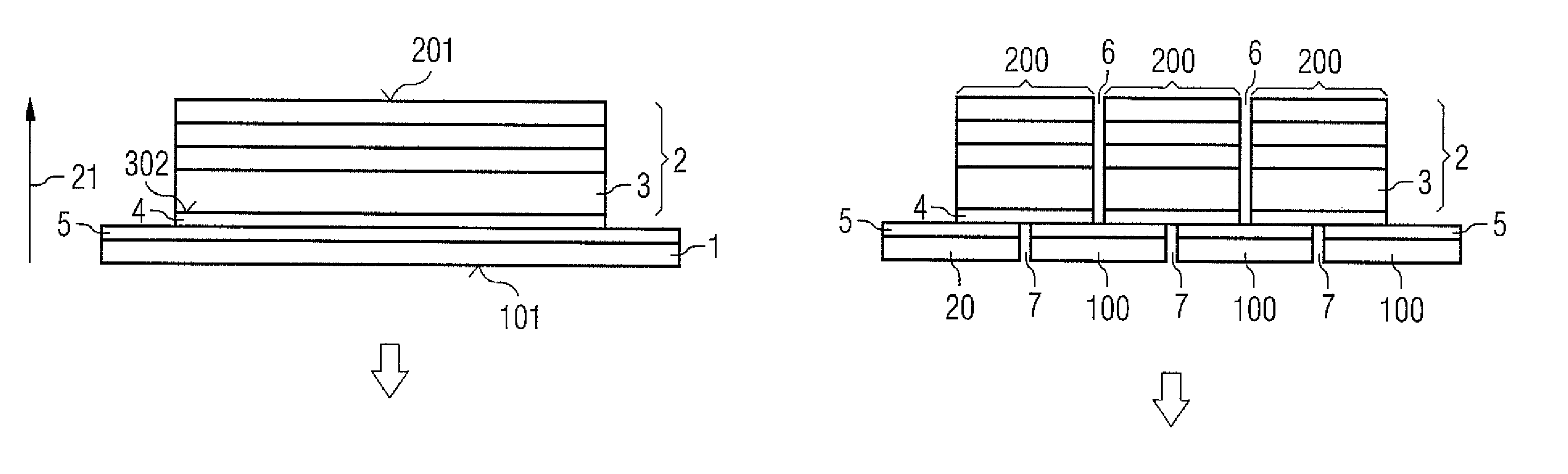
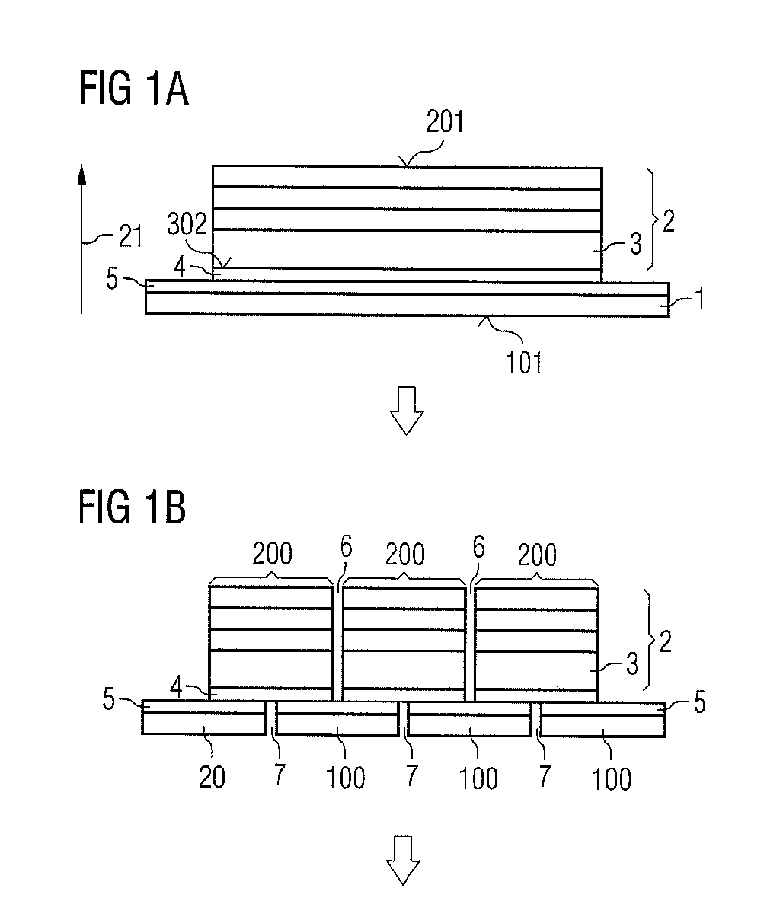
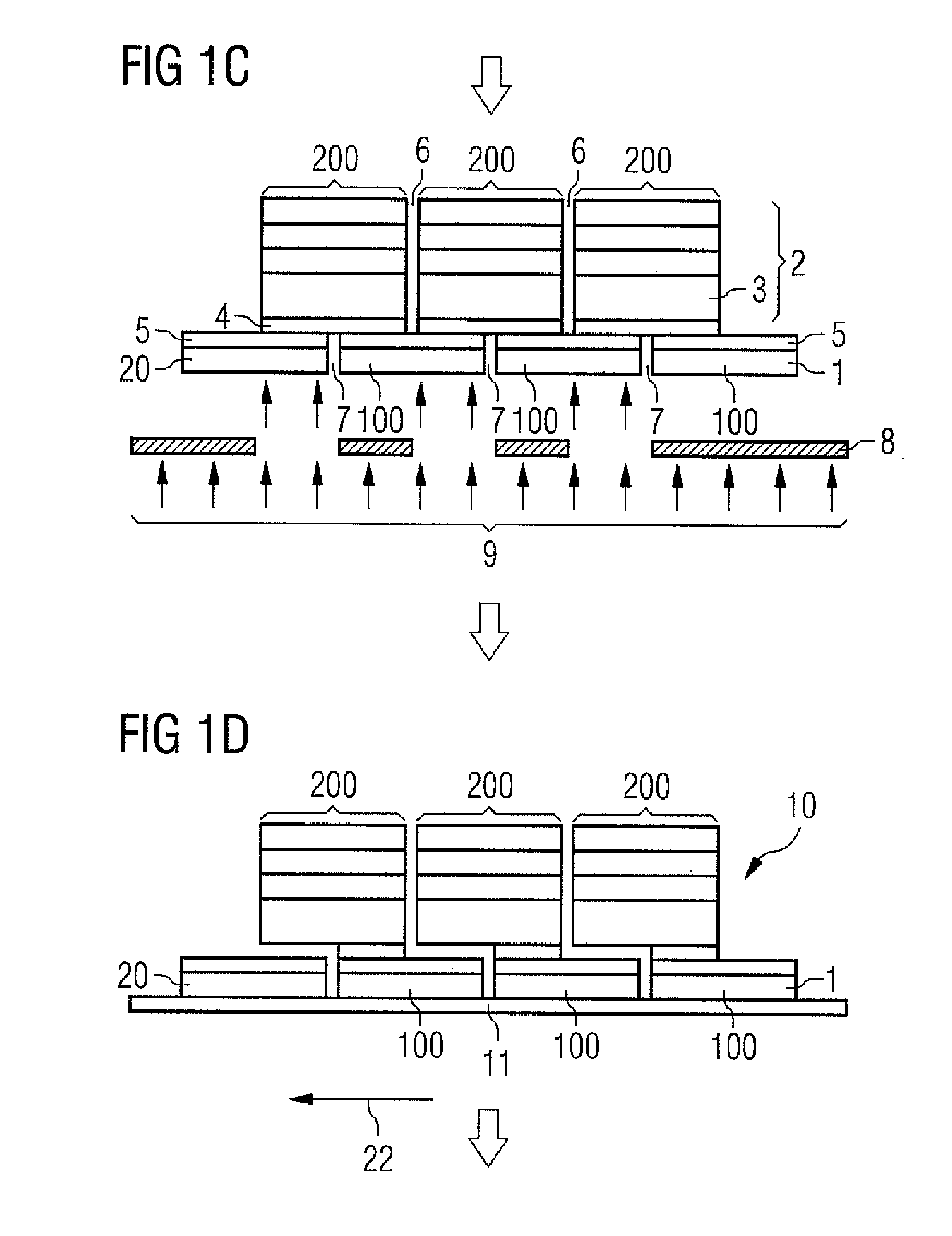
[0132]In the exemplary embodiments and figures, identical components and components having the same effect are each provided with the same reference symbols. The illustrated elements and their size ratios with respect to one another should in principle not be regarded as being true to scale and in fact individual elements, such as layers, may be illustrated with their size exaggerated in order to illustrate them better and / or to assist understanding.

[0133]In the exemplary embodiment of the method according to the invention of producing a plurality of radiation-emitting semiconductor bodies, as illustrated in FIGS. 1A to 1G, a semiconductor layer sequence 2 is provided which produces electromagnetic radiation during operation (cf. FIG. 1A).

[0134]By way of example, the semiconductor layer sequence 2 is based on GaN or some other nitride compound semiconductor material, and comprises a growth substrate wafer 3 on which the other layers of the semicon...


PUM


Abstract

A radiation-emitting semiconductor body with a carrier substrate and a method for producing the same. In the method, a structured connection is produced between a semiconductor layer sequence (2) and a carrier substrate wafer (1). The semiconductor layer sequence is subdivided into a plurality of semiconductor layer stacks (200) by means of cuts (6) through the semiconductor layer sequence, and the carrier substrate wafer (1) is subdivided into a plurality of carrier substrates (100) by means of cuts (7) through the carrier substrate wafer (1). In the method, the structured connection is formed in such a way that at least one semiconductor layer stack (200) is connected to one and only one associated carrier substrate (100). In addition, at least one cut (7) through the carrier substrate wafer is not extended by any of the cuts (6) through the semiconductor layer sequence such that a straight cut results through the carrier substrate wafer and the semiconductor layer sequence.

Description

RELATED APPLICATIONS[0001]This is a U.S. national stage under 35 USC §371 of application No. PCT / DE2007 / 000793, filed on May 3, 2007.[0002]This application claims the priority of German application no. 10 2006 020 537.5 filed May 3, 2006 and DE 10 2006 033 502.3 filed Jul. 19, 2006, the entire content of both of which is hereby incorporated by reference.FIELD OF THE INVENTION[0003]The invention relates to a radiation-emitting semiconductor body with a carrier substrate and a method for producing the same.[0004]In conventional methods for producing semiconductor bodies with a carrier substrate, a carrier substrate wafer and a semiconductor layer sequence are connected to one another over the entire area. Subdivision into individual semiconductor bodies is then possible only by cuts through the semiconductor layer sequence and through the carrier substrate wafer, which cuts run such that the cuts through the semiconductor layer sequence and through the carrier substrate wafer which bo...

Claims


Application Information

Patent Timeline
IPC IPC(8): H01L21/00H01L33/00H01L33/42H01L33/62
CPCH01L33/0095H01L21/78H01L33/42H01L33/62H01L2924/0002H01L2924/00
Inventor HARLE, VOLKERSPIKA, ZELJKO
Owner OSRAM OPTO SEMICON GMBH & CO OHG
Why Eureka
Try Eureka