
System for testing an integrated circuit of a device and its method of use

a technology for integrated circuits and devices, applied in the field of systems for testing integrated circuits of devices and their methods of use, to achieve the effect of improving the planarity of a surfa

Active Publication Date: 2011-10-04
AEHR TEST SYST
View PDF10 Cites 30 Cited by
  • Summary
  • Abstract
  • Description
  • Claims
  • Application Information

AI Technical Summary

Benefits of technology

This approach allows for effective testing of integrated circuits on unsingulated wafers by efficiently making and breaking contacts, reducing the complexity of full-wafer testing and enabling reliable identification of defects during early manufacturing stages.

Problems solved by technology

One challenge in full-wafer testing is that there are a large amount of contacts on a wafer and that a large number of power, ground, and signal connections thus have to be made.

Method used


Image

  • System for testing an integrated circuit of a device and its method of use
  • System for testing an integrated circuit of a device and its method of use
  • System for testing an integrated circuit of a device and its method of use

Examples


Embodiment Construction

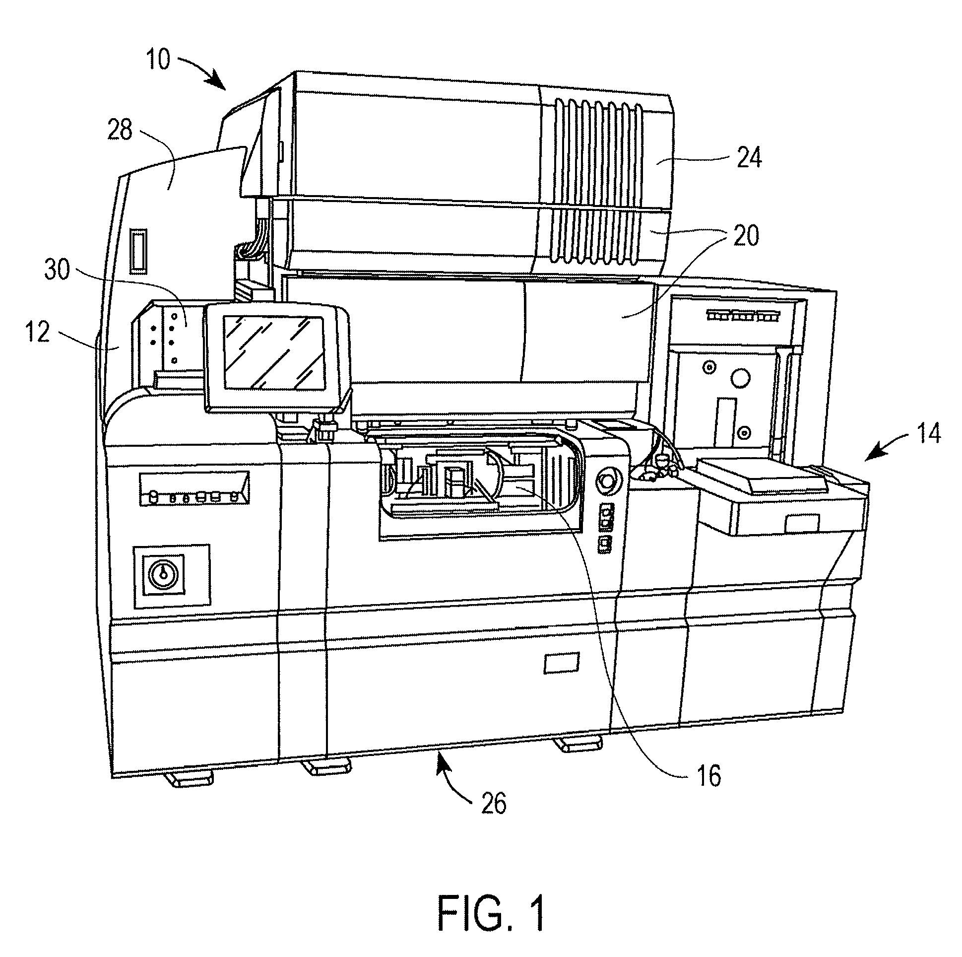
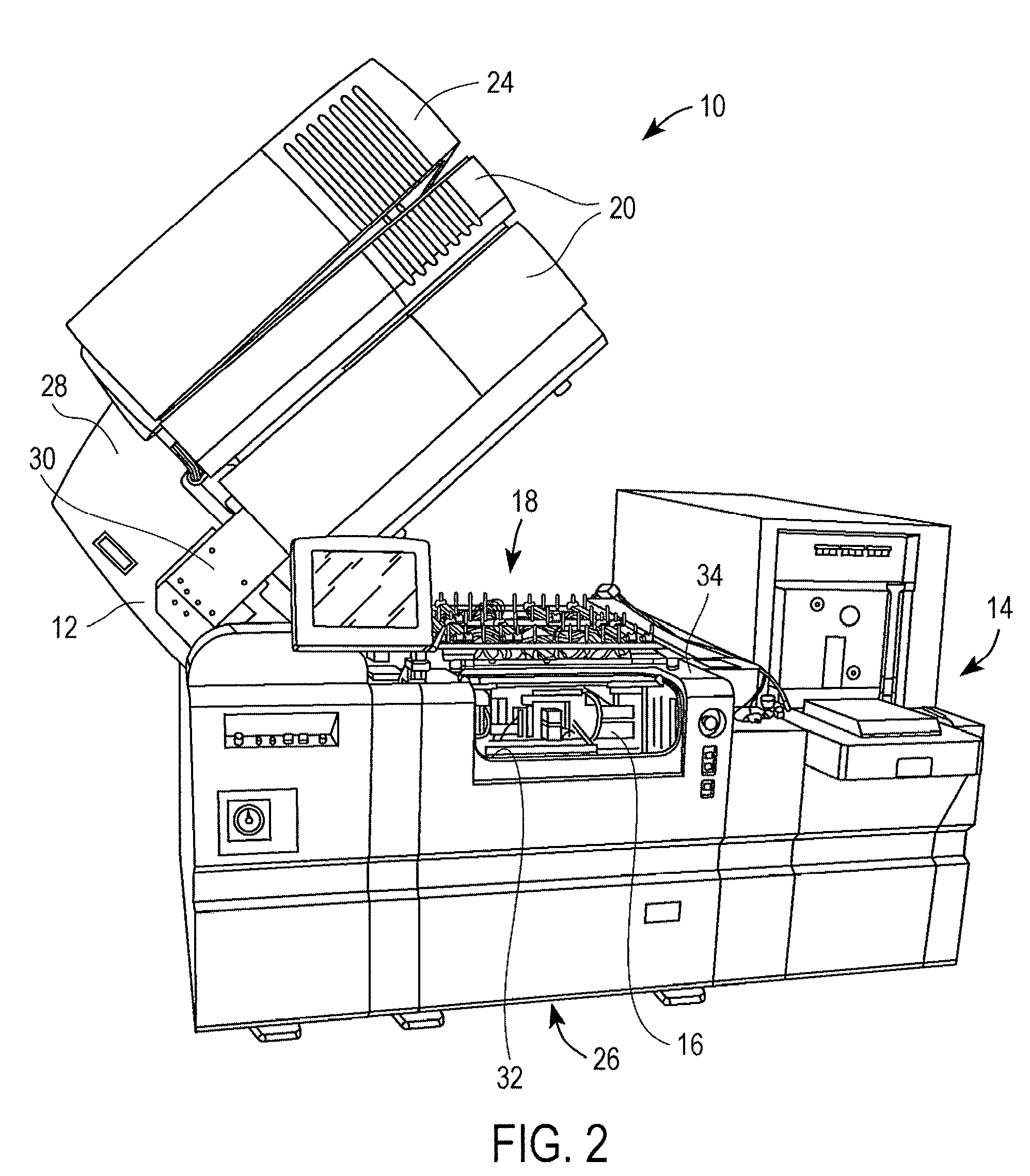
[0120]FIGS. 1 and 2 of the accompanying drawings illustrate an apparatus 10, which is particularly suitable for full-wafer testing of microelectronic circuits of unsingulated wafers and / or burn-in testing of unsingulated wafers and / or built-in self-testing of unsingulated wafers. The apparatus 10 includes a frame 12 and a number of modules mounted to the frame 12 including a wafer loader 14, a probing subassembly 16, a cartridge 18, a test head 20, and a thermal system 24.

[0121]The frame 12 has a prober base portion 26, a thermal system frame portion 28, and a test head frame portion 30. The thermal system frame portion 28 is pivotally mounted to the prober base portion 26. The test head frame portion 30 is pivotally mounted to the thermal system frame portion 28. The probing subassembly 16 and the cartridge 18 are mounted to lower and upper portions 32 and 34 respectively of the prober base portion 26, and the test head 20 and the thermal system 24 are mounted to the test head fram...


PUM


Abstract

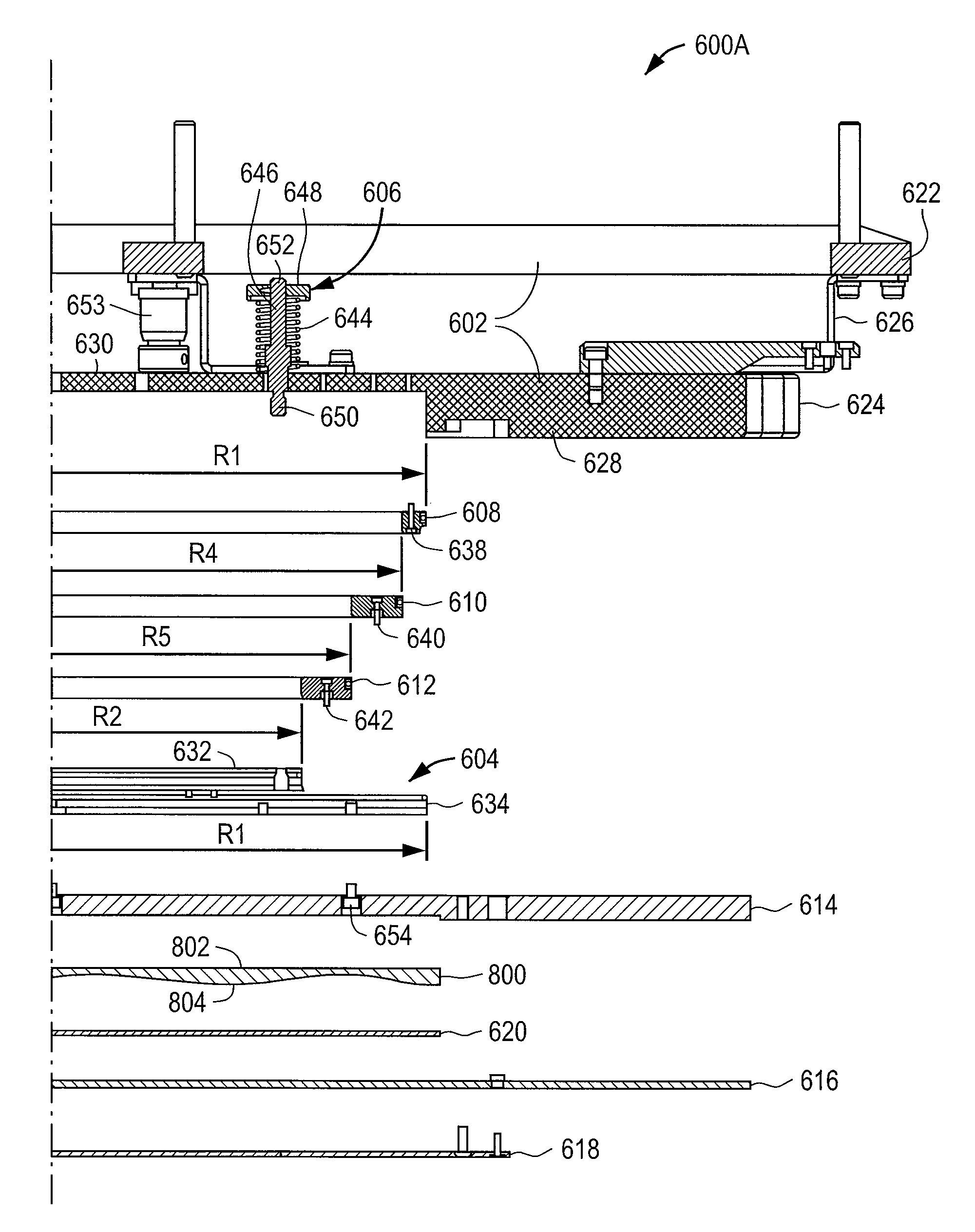
A method of testing an integrated circuit of a device is described. Air is allowed through a fluid line to modify a size of a volume defined between the first and second components of an actuator to move a contactor support structure relative to the apparatus and urge terminals on the contactor support structure against contacts on the device. Air is automatically released from the fluid line through a pressure relief valve when a pressure of the air in the fluid line reaches a predetermined value. The holder is moved relative to the apparatus frame to disengage the terminals from the contacts while maintaining the first and second components of the actuator in a substantially stationary relationship with one another. A connecting arrangement is provided including first and second connecting pieces with complementary interengaging formations that restricts movement of the contactor substrate relative to the distribution board substrate in a tangential direction.

Description

BACKGROUND OF THE INVENTION[0001]1). Field of the Invention[0002]This invention relates to an apparatus that is used for full-wafer testing and / or burn-in testing and / or built-in self-testing.[0003]2). Discussion of Related Art[0004]Microelectronic circuits are usually fabricated in and on semiconductor wafers. Such a wafer is subsequently “singulated” or “diced” into individual dies. Such a die is typically mounted to a supporting substrate for purposes of providing rigidity thereto and electronic communication with an integrated or microelectronic circuit of the die. Final packaging may include encapsulation of the die and the resulting package can then be shipped to a customer.[0005]It is required that the die or the package be tested before being shipped to a customer. Ideally, the die should be tested at an early stage for the purposes of identifying the defects that occur during early stage manufacturing.[0006]The earliest stage that a die can be tested is after completion of ...

Claims


Application Information

Patent Timeline
Patent Type & Authority Patents(United States)
IPC IPC(8): G01R1/067G01R31/20
CPCG01R31/2887G01R31/2886G01R31/2863G01R1/0491G01R1/06705G01R31/2601G01R31/2855G01R1/0416G01R1/0441G01R1/07307
Inventor LINDSEY, SCOTT E.YEH, JUNYJEJOVANOVIC, JOVANMALATHONG, SEANG P.
Owner AEHR TEST SYST
Learn More