
System for testing and sorting electronic components

a technology for electronic components and systems, applied in individual semiconductor device testing, semiconductor/solid-state device testing/measurement, instruments, etc., can solve the problems of reducing led sorting speed and throughput, and achieve the effect of increasing the overall throughput and speed

Active Publication Date: 2011-07-05
ASM ASSEMBLY AUTOMATION LTD
View PDF9 Cites 7 Cited by
  • Summary
  • Abstract
  • Description
  • Claims
  • Application Information

AI Technical Summary

Benefits of technology

[0007]It is thus an object of the invention to seek to provide a method and an apparatus for sorting electronic components having more common characteristics at a relatively higher sorting speed to achieve a higher overall throughput as compared to the conventional sorting systems described above.

Problems solved by technology

Thus, the resultant down-time reduces the LED sorting speed and throughput.

Method used


Image

  • System for testing and sorting electronic components
  • System for testing and sorting electronic components
  • System for testing and sorting electronic components

Examples


Embodiment Construction

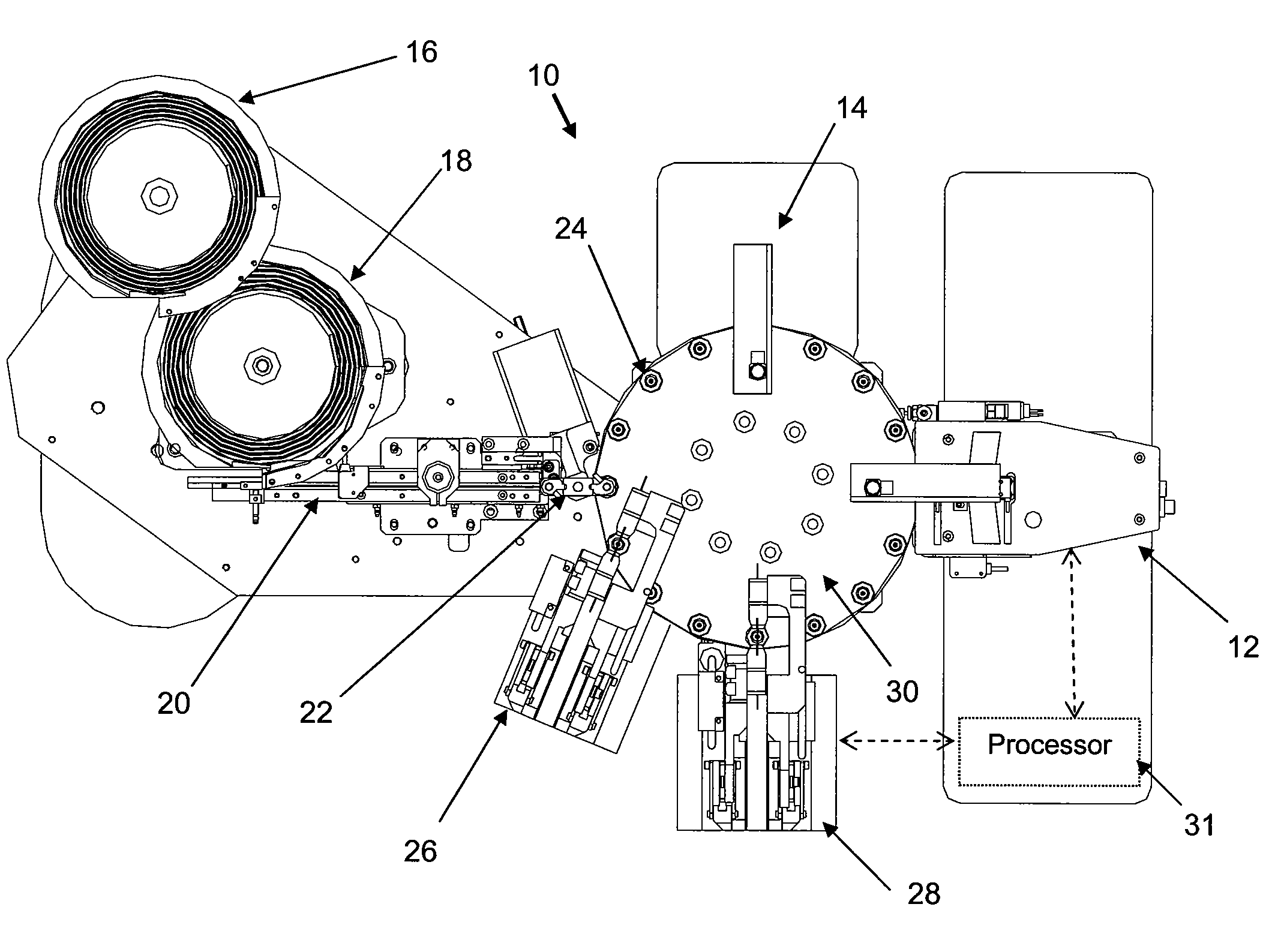
[0018]The preferred embodiment of the present invention will be described hereinafter with reference to the accompanying drawings.

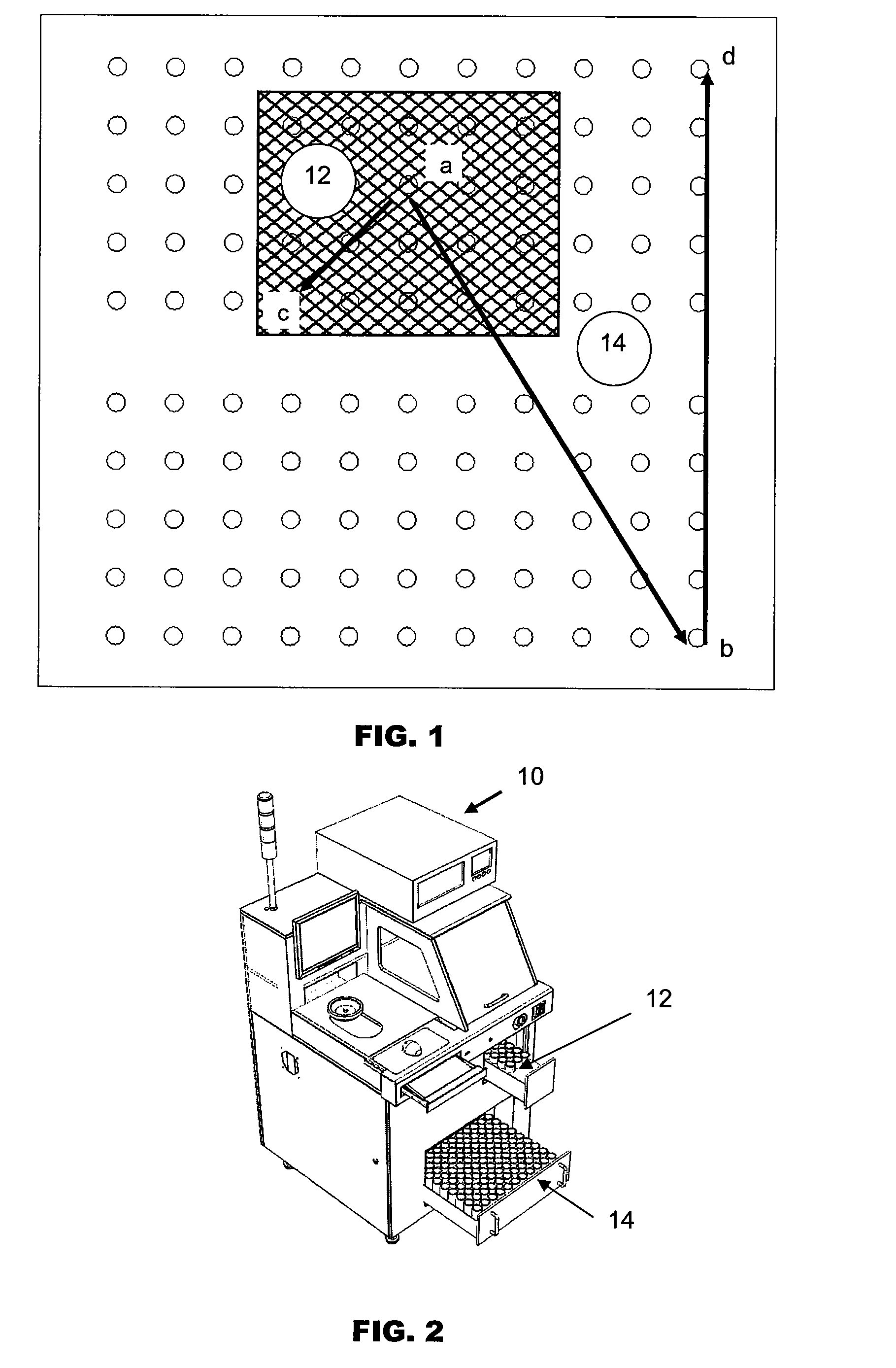
[0019]FIG. 1 is a schematic top view of a first tray, such as a high speed bin tray 12 according to the preferred embodiment of the invention, superimposed over a second tray, such as a normal bin tray 14. The high speed bin tray 12 and the normal bin tray 14 have receptacles in the form of bins for receiving tested electronic components, such as LEDs. This figure illustrates the advantage of arranging the bins that are more frequently used into the high speed bin tray 12. As the high speed bin tray 12 has fewer receptacles and is thus smaller than the normal bin tray 14, the motion distance and time taken for an output tube to move from bin a to bin c in the high speed bin tray 12 is shorter than from bin a to bin b. Thus, if a more frequently used bin at position b were to be consolidated into the high speed bin tray 12 at position c, a higher sorting s...


PUM


Abstract

A sorting system is provided for electronic components such as LED devices which includes a testing station for testing and determining a characteristic of each electronic component. A first tray has a plurality of receptacles for receiving tested electronic components and a second tray has more receptacles than the first tray for receiving tested electronic components. Electronic components comprising tested characteristics that occur with greater frequency are loaded into the receptacles of the first tray and electronic components comprising tested characteristics that occur with lower frequency are loaded into the receptacles of the second tray.

Description

FIELD OF THE INVENTION[0001]The present invention relates to a method and an apparatus for testing, and thereafter separating and sorting electronic components, such as light emitting diodes, according to the characteristics of the electronic components.BACKGROUND AND PRIOR ART[0002]A Light Emitting Diode (LED) is a display and lighting technology which is widely used in electrical and electronic products on the market as LEDs use less power, have longer lifetimes and produce little heat as compared to traditional incandescent light bulbs, as well as emit colored light. After assembly of an LED, each LED is tested to determine its optical and electrical properties before being sorted according to its determined characteristics. Since the characteristics of the assembled LEDs vary widely, an elaborate sorting system is used to classify and separate them after assembly.[0003]In a conventional sorting system for LEDs, the LEDs are loaded onto a test handler. Characterization of LEDs is...

Claims


Application Information

Patent Timeline
Patent Type & Authority Patents(United States)
IPC IPC(8): B07C5/344
CPCG01R31/2893G01R31/2894Y10S414/135G01R31/26H01L22/00
Inventor TSAI, PEI WEISZE, CHAK TONGWONG, SAI KITYIP, FONG SHING
Owner ASM ASSEMBLY AUTOMATION LTD
Learn More