Driving device and method for plasma display panel

a technology of driving device and display panel, which is applied in the direction of instruments, static indicating devices, etc., can solve the problems of increasing switching load, increasing the amount of data voltage drop for data electrodes, and more prominent drawback

Inactive Publication Date: 2011-03-22
LG ELECTRONICS INC
View PDF18 Cites 2 Cited by
  • Summary
  • Abstract
  • Description
  • Claims
  • Application Information

AI Technical Summary

Benefits of technology

[0020]Another object of the present invention is to provide a driving device and method for a plasma display panel in which when the plasma display panel is driven, the sustain periods are varied depending on certain characteristics, thereby providing a stable discharge characteristic without an erroneous discharge.
[0028]The present invention has an effect in that when the plasma display panel is driven, a recovery period of a data pulse voltage is sufficiently provided in the sustain period to provide a stable discharge characteristic at each of the sub-fields without an erroneous discharge where the discharge of the discharge cell is turned off.

Problems solved by technology

This creates a drawback in that the erroneous discharge is generated due to the jittering such as a case where the address discharge is not sufficiently generated only with an exterior predetermined data voltage at the address period of the next sub-field since the drop of the data voltage is not sufficiently recovered during the sustain period.
In particular, this drawback is more prominent in the PDP using a single scan method.
In the PDP using the single scan method, the switching load increases due to a longer line length of the data electrodes, which in turn causes an increase in the amount of data voltage drop for the data electrodes.
Also there is a drawback in that when the PDP is driven at a high temperature, the erroneous discharge is easily caused due to the loss of the wall charge, because a motion of a spatial charge is activated within the cell and a recombination is easily generated.

Method used


Image

  • Driving device and method for plasma display panel
  • Driving device and method for plasma display panel
  • Driving device and method for plasma display panel

Examples


Embodiment Construction

[0037]Preferred embodiments of the present invention will be described in a more detailed manner with reference to the drawings.

[0038]FIGS. 6a and 6b are views illustrating a data voltage characteristic and a waveform for describing a driving method for a plasma display panel according to the present invention.

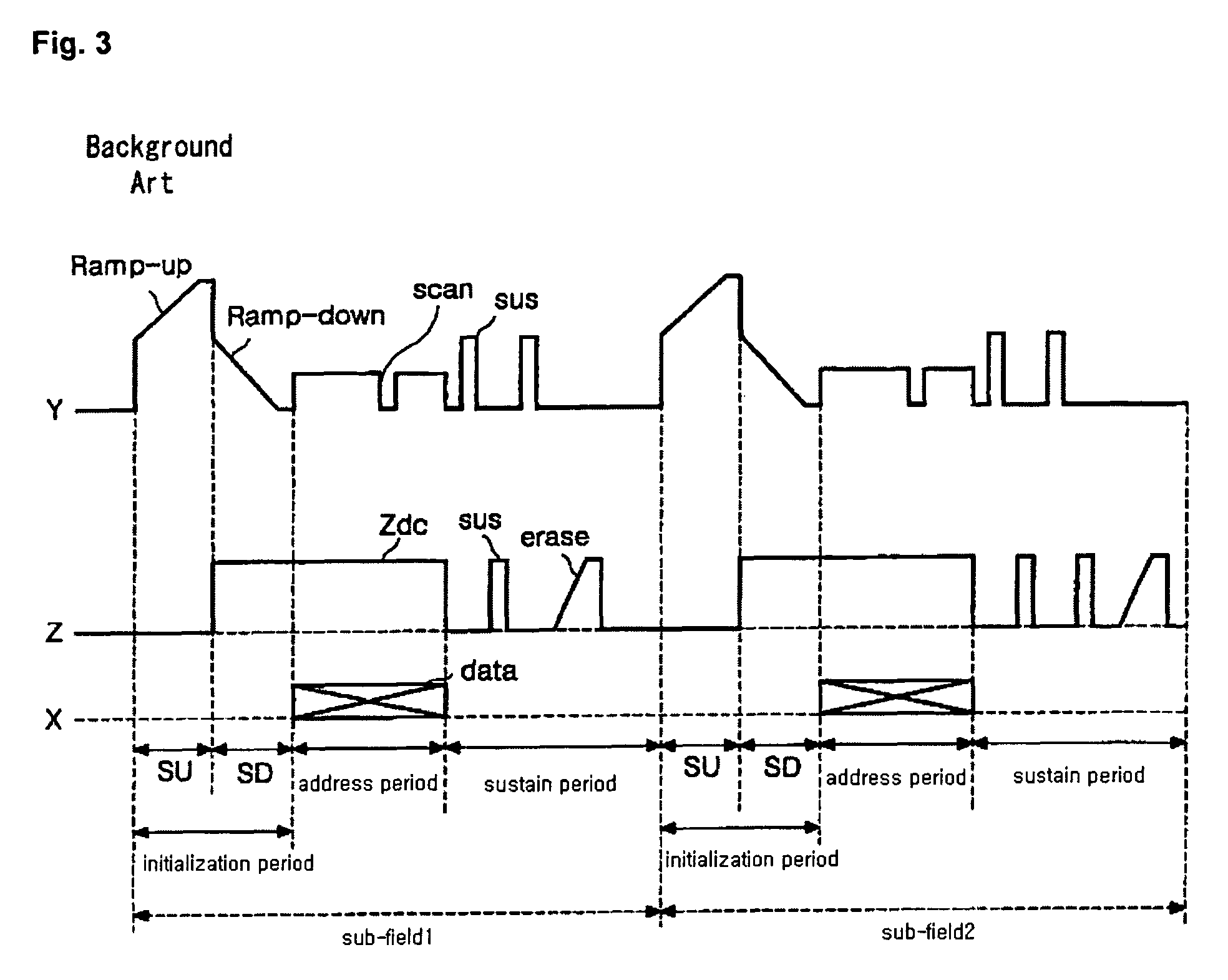
[0039]Referring to FIGS. 6a and 6b, the plasma display panel is driven by dividing each sub-field of a frame into a reset / initialization period for initializing an entire picture, an address period for selecting a cell, and a sustain period for sustaining the discharge of the selected cell.

[0040]At a setup period (SU) of the reset period, a ramp-up waveform (Ramp-up) is concurrently supplied to all scan electrodes (Y). At the same time, 0 [V] is supplied to a sustain electrode (Z) and an address electrode (X). The ramp-up waveform causes a write dark discharge not almost generating light between the scan electrode (Y) and the address electrode (X) and between the scan electrod...


PUM


Abstract

A plasma display apparatus and a method of driving the plasma display apparatus are provided. According to an embodiment, the plasma display apparatus is driven by dividing a sub-field into at least an address period and a sustain period. The apparatus includes a timing controlling unit to vary a length of the sustain period according to a data pattern associated with at least one address electrode.

Description

[0001]This Nonprovisional application claims priority under 35 U.S.C. §119(a) on Patent Application No. 10-2004-0096019 filed in Korea on Nov. 22, 2004, the entire contents of which are hereby incorporated by reference.BACKGROUND OF THE INVENTION[0002]1. Field of the Invention[0003]The present invention relates to a driving device and method for a plasma display panel (PDP), and more particularly, to a PDD including a driving device and using a driving method to recover a data voltage drop component occurring in an address discharge.[0004]2. Description of the Background Art[0005]Plasma display panel (PDP) displays a picture including a character or a graphic by exciting a phosphor using an ultraviolet ray of 147 nm, which is generated when an inert mixture gas such as He+Xe, Ne+Xe, or He+Ne+Xe is discharged.[0006]FIG. 1 is a view illustrating a three-electrode alternate current surface discharge type PDP according to the background art. Referring to FIG. 1, the three-electrode alte...

Claims


Application Information

Patent Timeline
Patent Type & Authority Patents(United States)
IPC IPC(8): G09G3/28G09G3/20G09G3/292G09G3/288G09G3/291G09G3/293G09G3/294G09G3/296G09G3/298
CPCG09G3/2942G09G3/2022G09G3/2922G09G3/298G09G2310/0275G09G2320/0233G09G2320/0238G09G2320/0247G09G3/294G09G3/296
Inventor JUNG, YUN KWONWOO, SEUNG WOO
Owner LG ELECTRONICS INC
Why Eureka
Try Eureka