
Interfacing at low temperature using CMOS technology

a low temperature, cmos technology, applied in the direction of pulse generators, instruments, pulse techniques, etc., can solve the problems of unsuitable use for control of quantum circuits, not usually practical to produce cmos circuits of even modest complexity in research laboratories, etc., to achieve convenient interface, high unity-gain frequency, and high temporal control

Active Publication Date: 2011-03-22
NEWSOUTH INNOVATIONS PTY LTD
View PDF2 Cites 7 Cited by
  • Summary
  • Abstract
  • Description
  • Claims
  • Application Information

AI Technical Summary

Benefits of technology

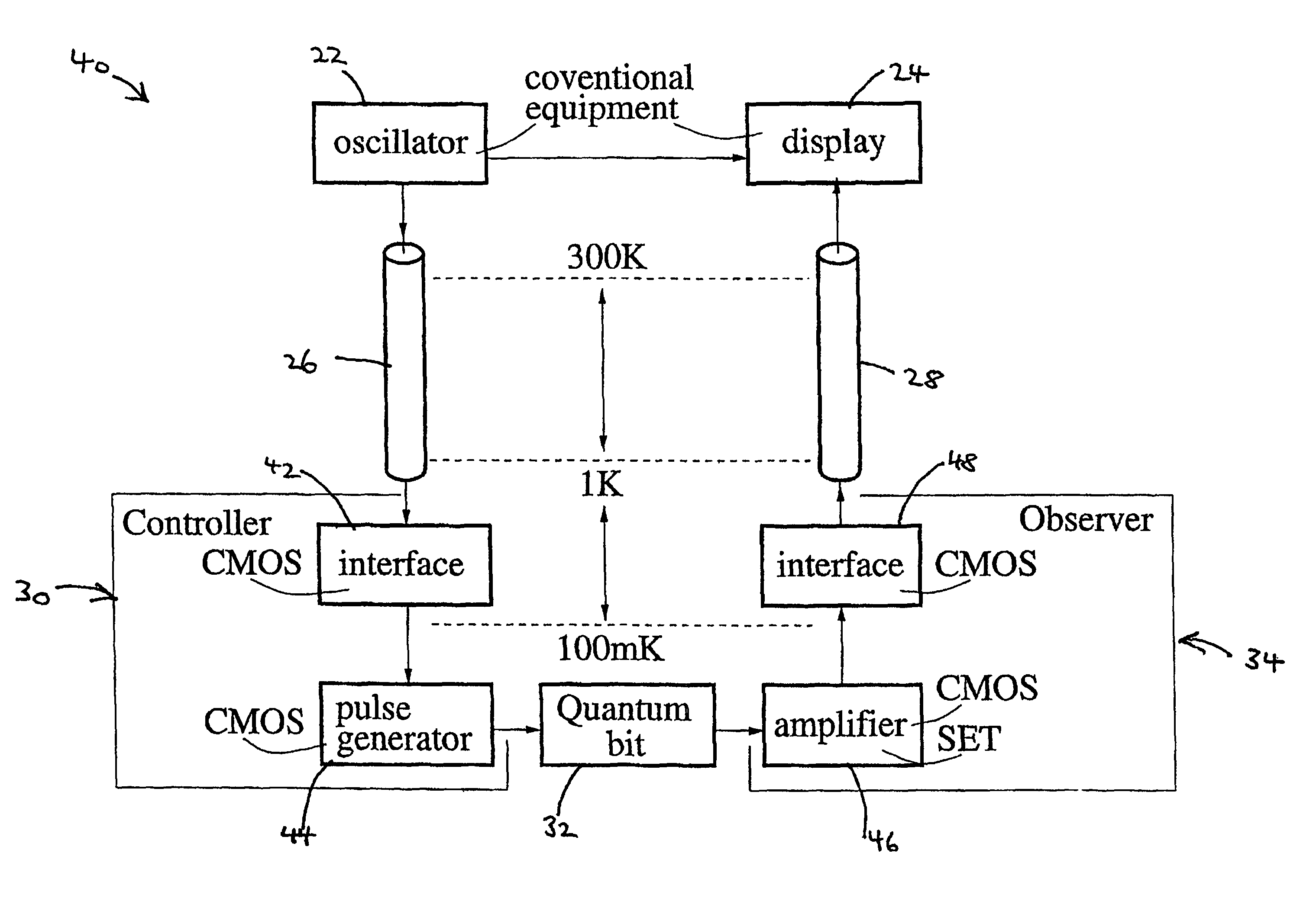
[0011]The high pulse-voltage swing (±500 mV) is available in MOS technology. Ultra-low power operation is due to the low parasitics of SOI devices. In addition there is high capacitive drivability and scalability available in this technology. These features provide important advantages, particularly for qubit control, relative to other competing technologies such as RSFQ [3] which can only produce pulse-voltage swings of ˜10 mV.
[0012]Further advantages are large scale integration, and wide commercial availability. In fact, it has been found that the invention can be designed and built using a suitable SOI-CMOS process that was developed particularly for radio-frequency (RF) applications developed at a commercial foundry.
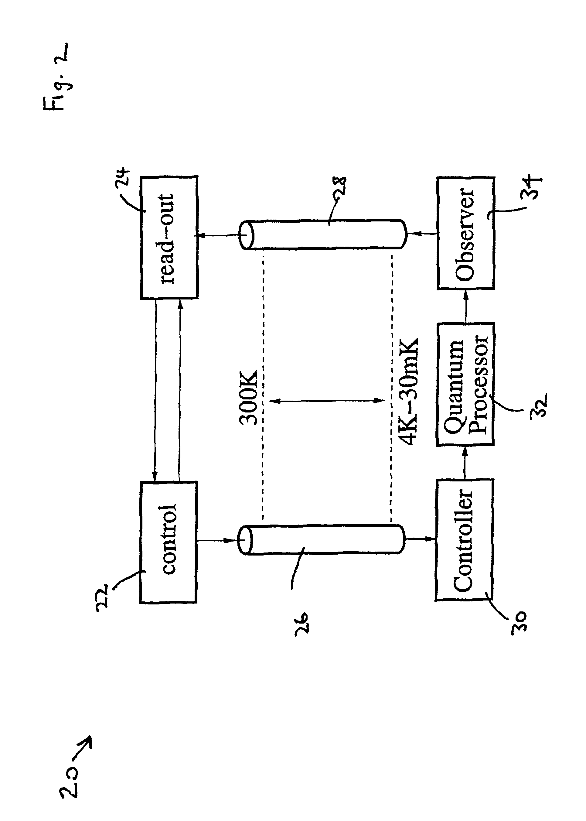
[0016]The SOI-CMOS circuits of the invention, because of their high unity-gain frequency (ft), may be used to generate voltage or current pulses with rapid pulse-edge transition times, or generalized voltage or current waveforms with high temporal control. Such high-bandwidth waveform generators may be used to control other circuits or systems that require low temperatures for their operation. Because the SOI-CMOS circuits of the invention can operate at low temperatures, it is possible for them to be conveniently interfaced with the circuits or systems being controlled, with minimal corruption or distortion of the controlling voltage or current waveform.
[0017]The SOI-CMOS circuits of the invention, because of their high unity-gain frequency (ft), may be also used as high-bandwidth, voltage or current amplifiers. Such high-bandwidth amplifiers may be used to observe (i.e. measure) other circuits or systems that require low or ultra-low temperatures for their operation. Because the SOI-CMOS circuits of the invention can operate at low temperatures, it is possible for them to be conveniently interfaced with the circuits or systems being observed (measured), with a high signal-to-noise ratio and without losing high-frequency information.
[0019]In addition the controller circuits of the invention are able to provide duty-cycle (dwell time) controlled rapid single-shot pulses suitable for qubit control.

Problems solved by technology

Others have integrated commercial CMOS processes with superconducting technologies [11-13], which has led them to characterize those MOSFETs at 4.2 K. However, it is quite commonly documented that MOSFET channels may freeze-out at cryogenic temperatures [11], [12] rendering them unsuitable for use for control of quantum circuits.
Additionally, it is not usually practical to produce CMOS circuits of even modest complexity in a research laboratory; but only in a commercial foundry.

Method used


Image

  • Interfacing at low temperature using CMOS technology
  • Interfacing at low temperature using CMOS technology
  • Interfacing at low temperature using CMOS technology

Examples


Embodiment Construction

Part 1

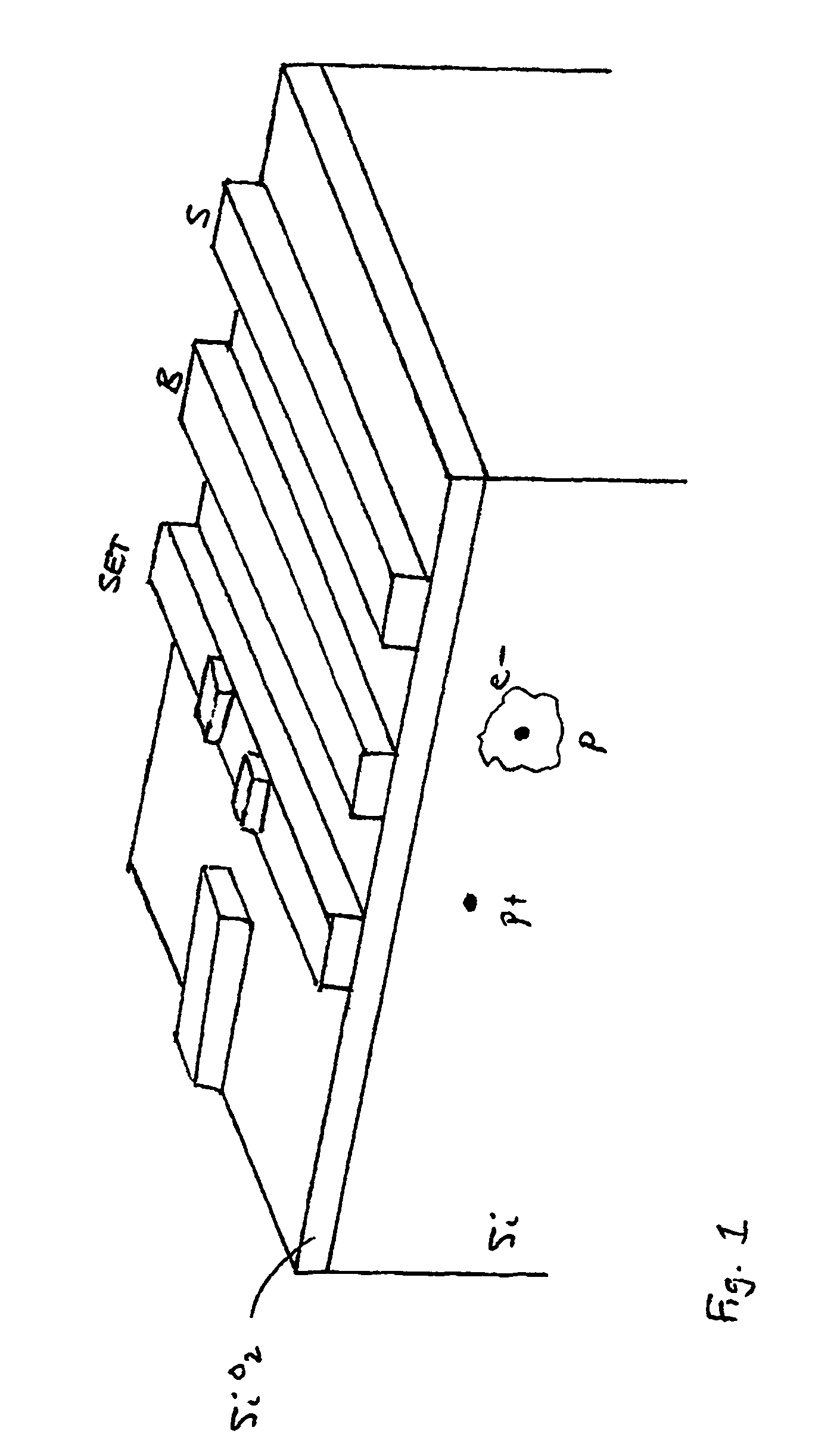
[0039]This example concerns the control and readout for a silicon (Si) based quantum computer. A quantum binary digit (qubit) is the fundamental computational element of the quantum computer. The solid-state qubit can be either a spin qubit [1], or a charge qubit [2]. In this example we consider a silicon charge qubit, however, we note that silicon spin-based qubits are expected to have much longer quantum coherence times and would be the preferred choice in most cases.

[0040]A buried donor charge qubit is shown in FIG. 1 for the case of P dopants in Si, although a number of other dopant-substrate systems could also be considered. The lowest two states of a single electron localized by the double well formed by two donor P+ ions give rise to a natural identification of the quantum logic states. External control over the barrier height and potential offset (or symmetry) is facilitated by B and S gates, respectively, placed about the buried (P-P+) system. With appropriate negativ...


PUM


Abstract

This invention concerns interfacing to electronic circuits or systems operating at low temperature or ultra-low temperature using complementary metal-oxide semiconductor (CMOS) technology. Low temperature in this case refers to cryogenic temperatures in particular, but not exclusively, to the 4.2 K region. Ultra-low temperatures here refers to the sub-1 K range, usually accessed using dilution refrigerator systems. The electronic circuits comprise a controller (for writing and manipulation), an observer (for readout and measurement) circuits, or both, fabricated from ultra-thin silicon-on-insulator (SOI) CMOS technology.

Description

TECHNICAL FIELD[0001]This invention concerns interfacing to electronic circuits or systems, such as integrated circuits, operating at low temperature using complementary metal-oxide semiconductor (CMOS) technology. Low temperature in this case refers to cryogenic temperatures, in particular but not exclusively to the 4.2 K region. Ultra-low temperatures here refers to the sub 1 K range, usually accessed using dilution refrigerator systems.BACKGROUND ART[0002]Electronic components in general, such as bipolar transistors will not work at low temperatures, below about 70 K.[0003]Complementary metal-oxide semiconductor, technology (CMOS) was originally developed for room-temperature low-power applications.[0004]Although much domestic and commercial electronics operate at room temperature (300 K) there are an important and growing number of applications which require lower temperatures.[0005]It has been known for some decades that metal-oxide-semiconductor field-effect transistors (MOSFE...

Claims


Application Information

Patent Timeline
Patent Type & Authority Patents(United States)
IPC IPC(8): H01L25/00G06N99/00
CPCH03K3/38H01L2924/0002H01L2924/00
Inventor DZURAK, ANDREW STEVENEKANAYAKE, SOBHATH RAMESHCLARK, ROBERT GRAHAMLEHMANN, TORSTEN
Owner NEWSOUTH INNOVATIONS PTY LTD
Learn More