Electrophotographic photoreceptor

a photoreceptor and electron beam technology, applied in the field of electron beam photoreceptors, can solve the problems of difficult crystal deposition during the preparation of the photosensitive layer, difficult to render the image, etc., and achieve the effect of reducing image defects

Inactive Publication Date: 2011-02-01
KONICA MINOLTA BUSINESS TECH INC
View PDF3 Cites 0 Cited by
  • Summary
  • Abstract
  • Description
  • Claims
  • Application Information

AI Technical Summary

Benefits of technology

[0005]It is an object of the invention to provide an electrophotographic photoreceptor which is uniform without causing deposition of a charge transport material, and exhibiting no black-spot defects with minimized image defects due to filming.

Problems solved by technology

However, structurally symmetrical N,N′-bis-(4-methylphenyl)-N,N′-bisphenyl-1,1′-biphenyl-4,4′-diamine, which is superior in electric characteristics such as sensitivity, exhibits high crystallinity and crystal deposition during preparation of the photosensitive layer, rendering difficult the use thereof.
Since such structurally symmetrical N,N′-bis-(4-methylphenyl)-N,N′-bisphenyl-1,1′-biphenyl-4,4′-diamine is superior in electric characteristics such as sensitivity, there was attempted preparation of a charge transport layer not exhibiting the foregoing defect but it was difficult to prevent crystal deposition during preparation of the photosensitive layer.

Method used


Image

  • Electrophotographic photoreceptor
  • Electrophotographic photoreceptor
  • Electrophotographic photoreceptor

Examples


examples

[0074]The present invention will be described with reference to examples but is by no means limited to these. In Examples, “part(s)” represents parts by mass, unless otherwise noted.

Preparation of N-Type Semiconductor Particles

[0075]In 10 parts of a mixture of ethanol / n-propyl alcohol / THF (45:20:35 by volume) was dissolved 0.1 parts of copolymer of methylhydrogen-siloxane and dimethylsiloxane (1:1). Further thereto was added 3.5 parts of rutile type titanium dioxide (having a number average primary particle size of 35 nm and having been subjected to a 5% alumina primary surface treatment by alumina), stirred for 1 hr. to perform a surface treatment (secondary treatment) and separated from the solvents. There was titanium oxide particle 1 as surface treated N-type semiconductor particles.

[0076]Titanium oxides 2 and 3 were each prepared similarly to the foregoing titanium oxide 1, except that the number average primary particle size was changed to 3 and 100 nm, respectively.

Preparatio...


PUM

PropertyMeasurementUnit
number average primary particle sizeaaaaaaaaaa
particle sizeaaaaaaaaaa

Abstract

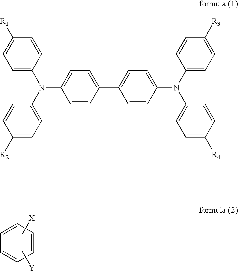
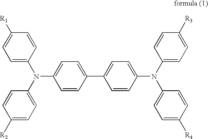
An electrophotographic photoreceptor is disclosed, comprising on an electrically conductive support an intermediate layer, a charge generation layer and a charge transport layer in this order, wherein the charge transport layer contains a charge transport material represented by formula (1) and a compound represented by formula (2) and the content of the compound represented by formula (2) is not less than 100 ppm and not more than 5000 ppm.

Description

[0001]This application claims priority from Japanese Patent Application No. JP2006-233317 filed on Aug. 30, 2006, which is incorporated hereinto by reference.FIELD OF THE INVENTION[0002]The present invention relates to electrophotographic photoreceptors.BACKGROUND OF THE INVENTION[0003]There have been employed N,N,N′,N′-tetra(aryl)-1,1′-biphenyl-4,4′-diamines as a charge transport material, as disclosed in, for example, JP-B No. 63-6864 (hereinafter, the term JP-B refers to Japanese Patent Publication). However, structurally symmetrical N,N′-bis-(4-methylphenyl)-N,N′-bisphenyl-1,1′-biphenyl-4,4′-diamine, which is superior in electric characteristics such as sensitivity, exhibits high crystallinity and crystal deposition during preparation of the photosensitive layer, rendering difficult the use thereof. In practice, there have been mainly used N,N′-bis-(3-methylphenyl)-N,N′-bisphenyl-1,1′-biphenyl-4,4′-diamine, as disclosed in, for example, JP-A Nos. 2001-356500 and 2002-40687, or a...

Claims


Application Information

Patent Timeline
Patent Type & Authority Patents(United States)
IPC IPC(8): G03G5/047
CPCG03G5/047G03G5/0517G03G5/0525G03G5/0614G03G5/14704G03G5/061443
Inventor SAKIMURA, TOMOOISHIE, MASAHIROYABUKI, SHINICHIMIWA, HIDAYA
Owner KONICA MINOLTA BUSINESS TECH INC
Why Eureka
Try Eureka