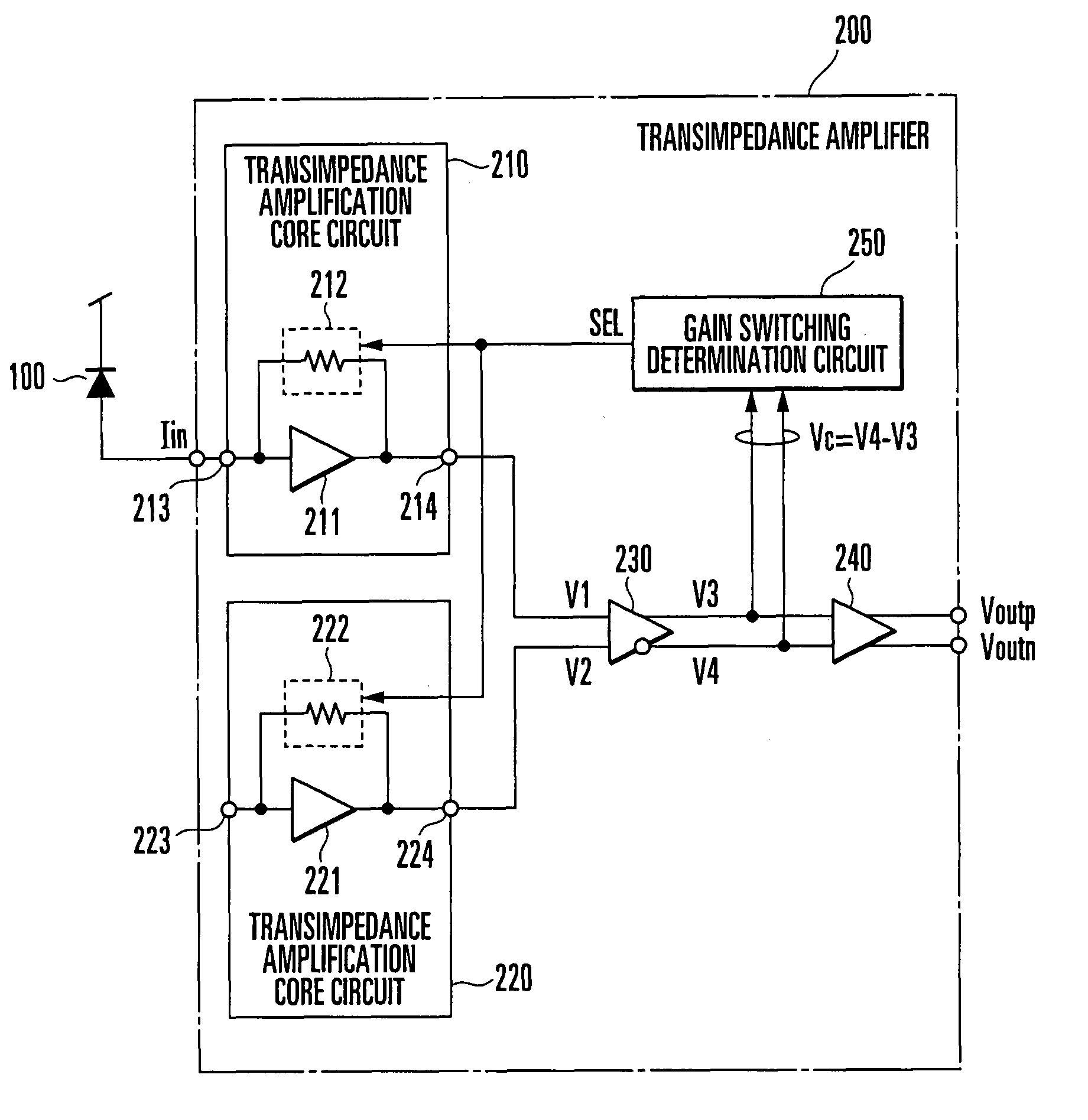
Transimpedance amplifier
a technology of transimpedance amplifier and amplifier, which is applied in the direction of electromagnetic transceivers, gain control, instruments, etc., can solve problems such as waveform distortion
- Summary
- Abstract
- Description
- Claims
- Application Information
AI Technical Summary
Benefits of technology
Problems solved by technology
Method used
Image
Examples
first embodiment
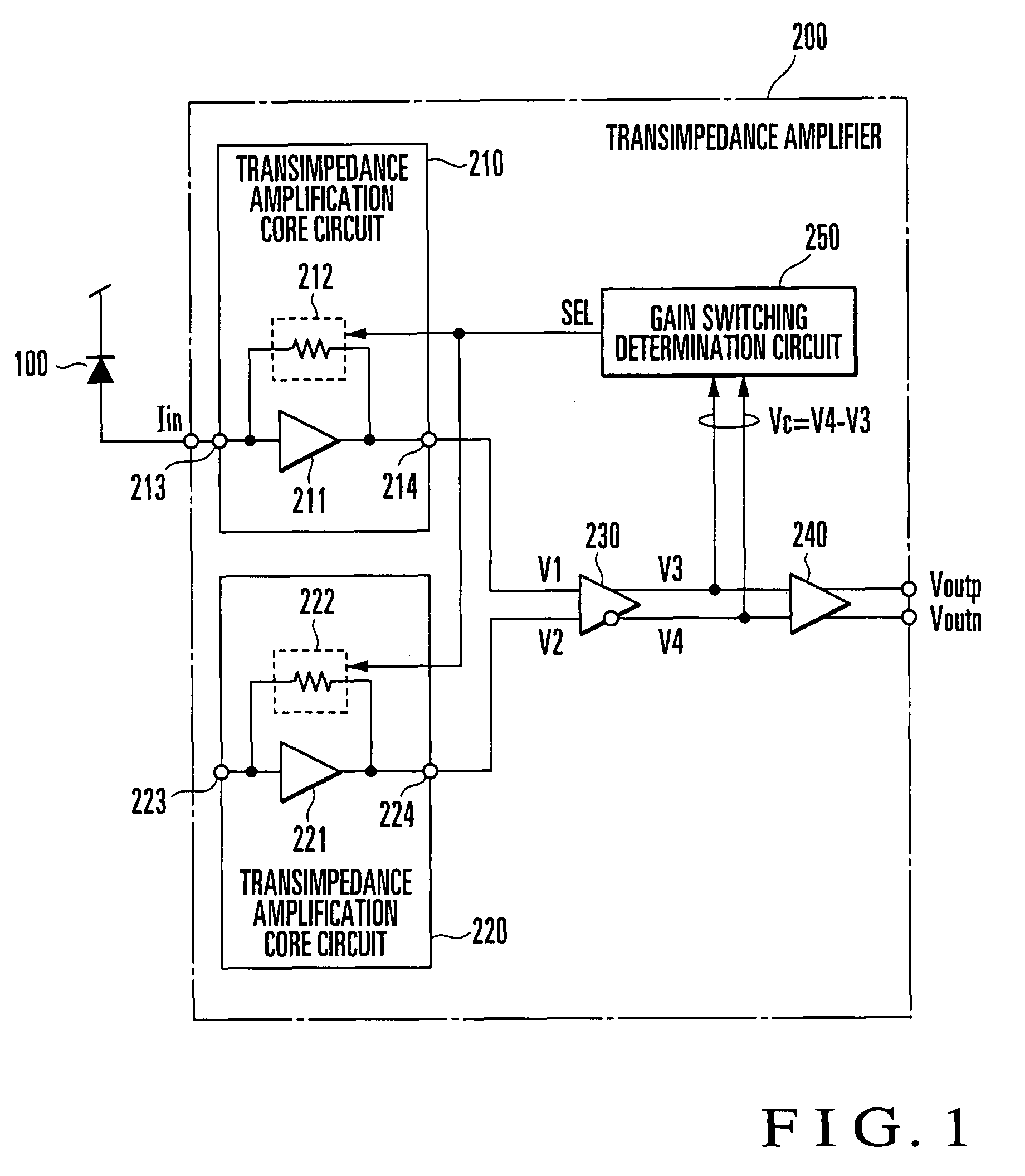
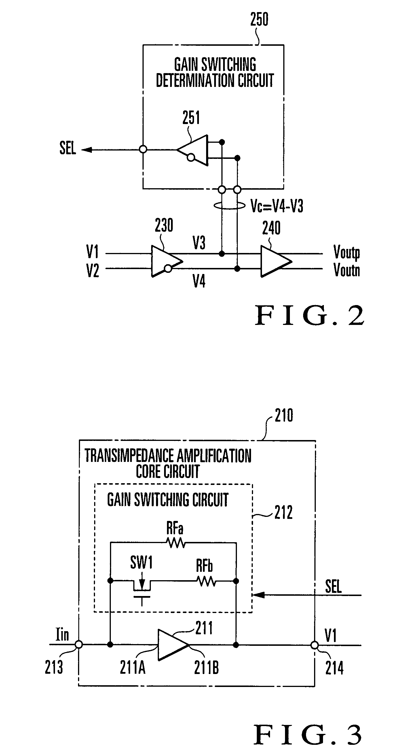
[0115]The arrangement of a transimpedance amplifier according to the first embodiment of the present invention will be described with reference to FIGS. 1 and 2.
[0116]In an optical transmission circuit such as an optical transmission system, optical interconnection, or passive optical network (OPN) system which can perform high-speed data transmission, an optical reception circuit which converts an optical signal received by a light-receiving element 100 and sent through an optical fiber into an electrical signal uses a transimpedance amplifier 200 shown in FIG. 1.
[0117]As shown in FIG. 1, the transimpedance amplifier 200 mainly comprises a first transimpedance amplifier core circuit 210, second transimpedance amplifier core circuit 220, inter-stage buffer circuit 230, output buffer circuit 240, and gain switching determination circuit 250.
[0118]The first transimpedance amplifier core circuit 210 includes an amplification circuit 211, gain switching circuit 212, input terminal 213, ...
second embodiment
[0152]The arrangement of a transimpedance amplifier according to the second embodiment of the present invention will be described next with reference to FIGS. 9 to 11. The same reference numerals as in FIGS. 2 to 4 denote the same components in FIGS. 9 to 11.
[0153]The first embodiment has exemplified the case wherein the gains of the transimpedance amplifier core circuits 210 and 220 are switched by one step between “high gain” and “low gain”. The second embodiment will exemplify a case wherein gains are switched by a plurality of steps, more specifically, a case wherein the gains of transimpedance amplifier core circuits 210 and 220 are switched by two steps between “high gain”, “intermediate gain”, and “low gain”. Note that the constituent elements of the transimpedance amplifier according to this embodiment are the same as those in the first embodiment except for a gain switching determination circuit and first and second transimpedance amplifier core circuits, and a detailed des...
third embodiment
[0172]A concrete example of a transimpedance amplifier core circuit used in a transimpedance amplifier according to the third embodiment of the present invention will be described next with reference to FIGS. 14 to 16.
[0173]Each of transimpedance amplifier core circuits 210B and 220B in FIG. 14 includes a transimpedance gain switching circuit 281 which switches transimpedance gains and an open loop gain switching circuit 282 which switches open loop gains as each of gain switching circuits 212B and 222B which switches the gains in two steps between “high gain”, “intermediate gain”, and “low gain”.
[0174]The transimpedance gain switching circuit 281 comprises feedback resistors RF1, RF2, and RF3 which determine a transimpedance gain and NMOS transistors NM1 and MN2 which operate as switches. The open loop gain switching circuit 282 comprises load resistors RL1, RL2, and RL3 which determine an open loop gain and NMOS transistors MN3 and MN4 which operate as switches. The NMOS transisto...
PUM
 Abstract
Description
Claims
Application Information
 - R&D
- Intellectual Property
- Life Sciences
- Materials
- Tech Scout
- Unparalleled Data Quality
- Higher Quality Content
- 60% Fewer Hallucinations
Browse by: Latest US Patents, China's latest patents, Technical Efficacy Thesaurus, Application Domain, Technology Topic, Popular Technical Reports.
© 2025 PatSnap. All rights reserved.Legal|Privacy policy|Modern Slavery Act Transparency Statement|Sitemap|About US| Contact US: help@patsnap.com


