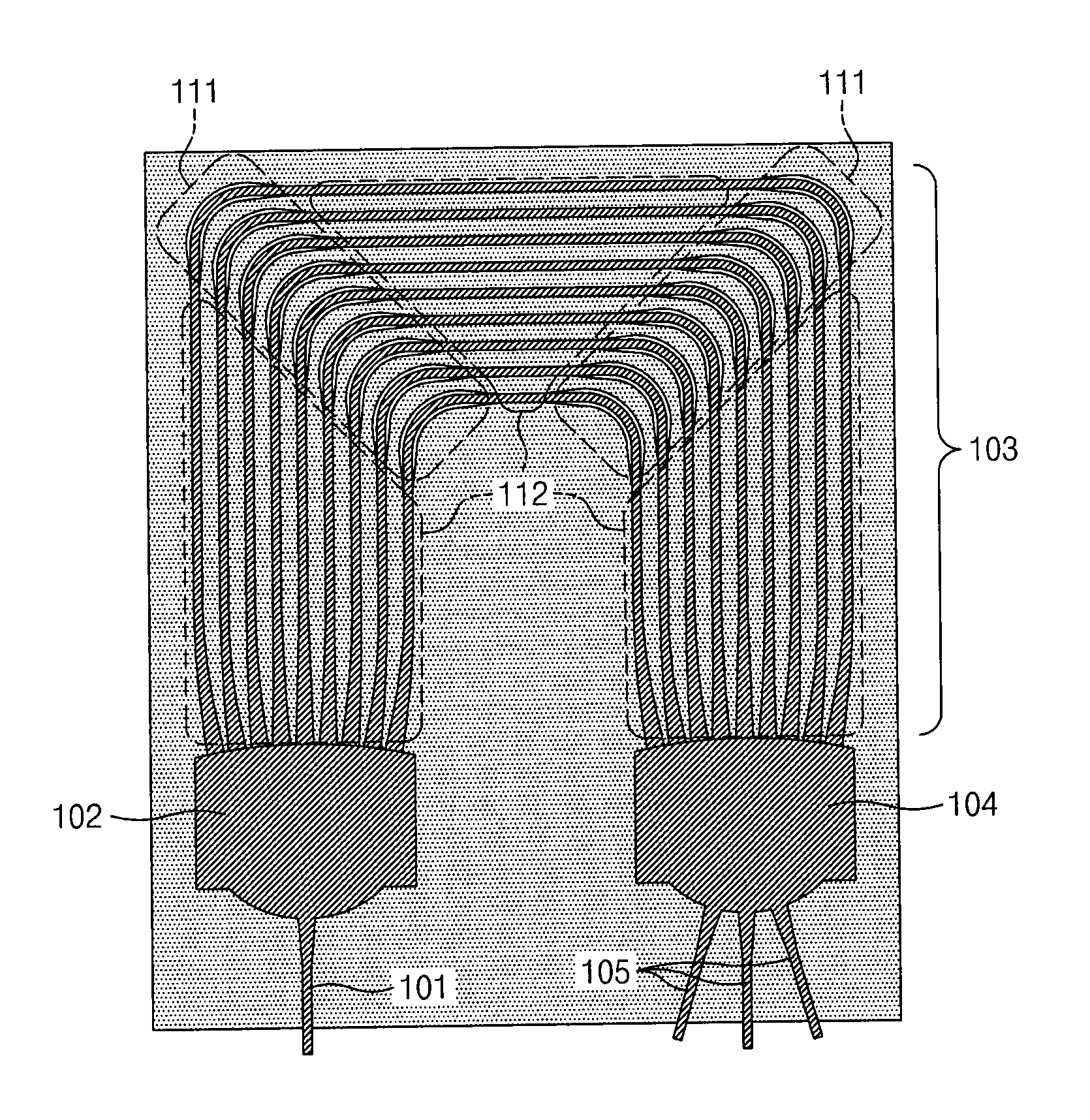
Waveguide structure and arrayed waveguide grating structure
a waveguide and array technology, applied in the field of photonic devices, can solve the problems that the method proposed by w. bogaerts et al. has limitations in reducing phase errors of arrayed waveguides, and achieve the effect of reducing coupling loss
- Summary
- Abstract
- Description
- Claims
- Application Information
AI Technical Summary
Benefits of technology
Problems solved by technology
Method used
Image


Examples
Embodiment Construction
[0029]Preferred embodiments of the present invention will be described below in more detail with reference to the accompanying drawings. The present invention may, however, be embodied in different forms and should not be construed as limited to the embodiments set forth herein. Rather, these embodiments are provided so that this disclosure will be thorough and complete, and will fully convey the scope of the present invention to those skilled in the art.
[0030]In the specification, the dimensions of layers and regions are exaggerated for clarity of illustration. It will also be understood that when a layer (or film) is referred to as being ‘on’ another layer or substrate, it can be directly on the other layer or substrate, or intervening layers may also be present. Also, though terms like a first, a second, and a third are used to describe various regions and layers in various embodiments of the present invention, the regions and the layers are not limited to these terms. These term...
PUM
 Abstract
Description
Claims
Application Information
 - Generate Ideas
- Intellectual Property
- Life Sciences
- Materials
- Tech Scout
- Unparalleled Data Quality
- Higher Quality Content
- 60% Fewer Hallucinations
Browse by: Latest US Patents, China's latest patents, Technical Efficacy Thesaurus, Application Domain, Technology Topic, Popular Technical Reports.
© 2025 PatSnap. All rights reserved.Legal|Privacy policy|Modern Slavery Act Transparency Statement|Sitemap|About US| Contact US: help@patsnap.com