
High forward current diodes for reverse write 3D cell

a reverse write and current diode technology, applied in the direction of diodes, digital storage, instruments, etc., can solve the problems of difficult fabrication and operation of three-terminal devices, difficult to achieve and complex solutions for achieving erasable or multi-state cells

Active Publication Date: 2010-11-09
SANDISK TECH LLC
View PDF60 Cites 56 Cited by
  • Summary
  • Abstract
  • Description
  • Claims
  • Application Information

AI Technical Summary

Problems solved by technology

Some solutions for achieving erasable or multi-state cells are complex.
These memory cells are three-terminal devices which are relatively difficult to fabricate and operate at the very small dimensions required for competitiveness in modern integrated circuits.
Chalcogenides are difficult to work with and can present challenges in most semiconductor production facilities.

Method used


Image

  • High forward current diodes for reverse write 3D cell
  • High forward current diodes for reverse write 3D cell
  • High forward current diodes for reverse write 3D cell

Examples


example

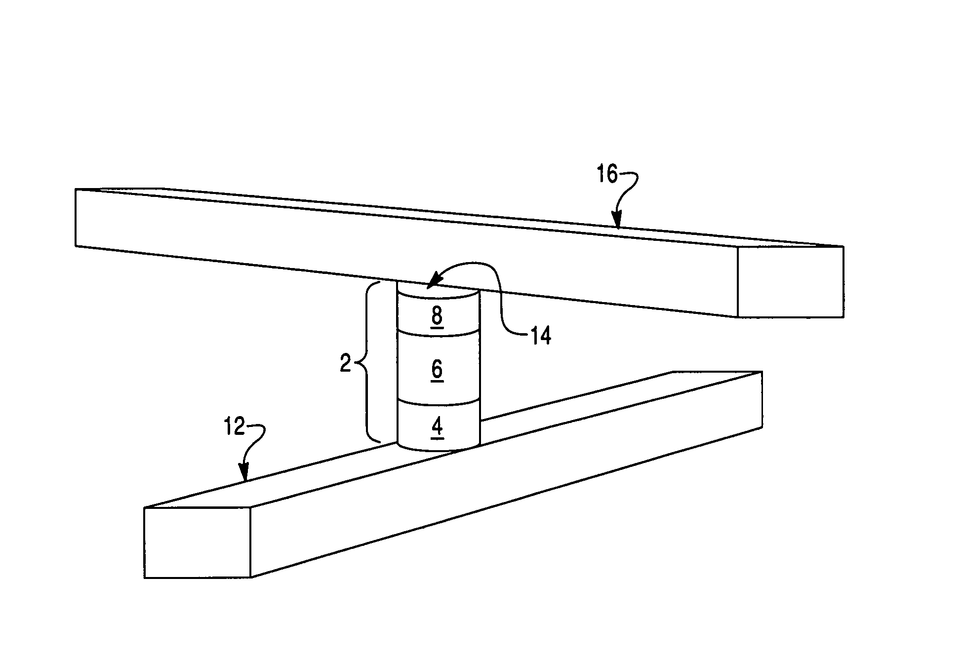
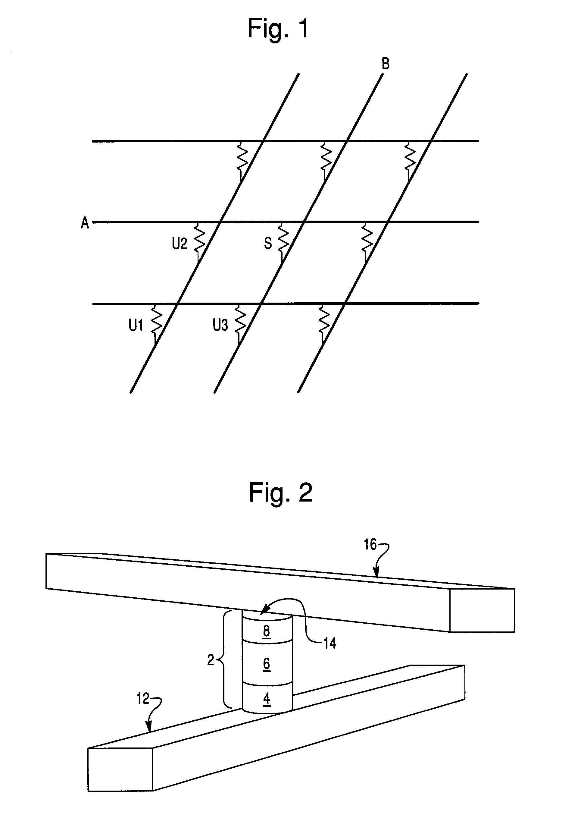
[0093]Fabrication of a single memory level will be described in detail. Additional memory levels can be stacked, each monolithically formed above the one below it. In this embodiment, a polycrystalline semiconductor diode will serve as the switchable memory element.

[0094]Turning to FIG. 15a, formation of the memory begins with a substrate 100. This substrate 100 can be any semiconducting substrate as known in the art, such as monocrystalline silicon, IV-IV compounds like silicon-germanium or silicon-germanium-carbon, III-V compounds, II-VII compounds, epitaxial layers over such substrates, or any other semiconducting material. The substrate may include integrated circuits fabricated therein.

[0095]An insulating layer 102 is formed over substrate 100. The insulating layer 102 can be silicon oxide, silicon nitride, high-dielectric film, Si—C—O—H film, or any other suitable insulating material.

[0096]The first conductors 200 are formed over the substrate and insulator. An adhesion layer ...


PUM


Abstract

A nonvolatile memory device includes at least one memory cell which comprises a diode and a metal oxide antifuse dielectric layer, and a first electrode and a second electrode electrically contacting the at least one memory cell. In use, the diode acts as a read / write element of the memory cell by switching from a first resistivity state to a second resistivity state different from the first resistivity state in response to an applied bias.

Description

BACKGROUND OF THE INVENTION[0001]This application is related to Herner, U.S. application Ser. No. 11 / 819,079, titled “METHOD OF MAKING HIGH FORWARD CURRENT DIODES FOR REVERSE WRITE 3D CELL” filed on the same day herewith, and hereby incorporated by reference in its entirety.[0002]The invention relates to a nonvolatile memory array.[0003]Nonvolatile memory arrays maintain their data even when power to the device is turned off. In one-time-programmable arrays, each memory cell is formed in an initial unprogrammed state, and can be converted to a programmed state. This change is permanent, and such cells are not erasable. In other types of memories, the memory cells are erasable, and can be rewritten many times.[0004]Cells may also vary in the number of data states each cell can achieve. A data state may be stored by altering some characteristic of the cell which can be detected, such as current flowing through the cell under a given applied voltage or the threshold voltage of a transi...

Claims


Application Information

Patent Timeline
Patent Type & Authority Patents(United States)
IPC IPC(8): G11C11/00G11C11/14
CPCG11C11/5692G11C13/003G11C13/0069G11C17/165H01L27/101H01L27/1021G11C17/16G11C2013/009G11C2213/33G11C2213/71G11C2213/72
Inventor HERNER, S. BRAD
Owner SANDISK TECH LLC
Learn More