Silicon carbide semiconductor device and method for manufacturing the same

a technology of silicon carbide and semiconductors, applied in the direction of semiconductors, semiconductor devices, electrical apparatus, etc., can solve the problems of silicon semiconductors not being suitable for use in such severe environments, power devices are sometimes required to operate in severe environments, and silicon power devices are now approaching the theoretical limit, etc., to achieve low resistance ohmic contact, improve switching characteristics, and reduce the effect of resistan

Inactive Publication Date: 2010-11-09
PANASONIC CORP
View PDF28 Cites 7 Cited by
  • Summary
  • Abstract
  • Description
  • Claims
  • Application Information

AI Technical Summary

Benefits of technology

[0045]According to the present invention, in a semiconductor device including an n-type impurity region and a p-type impurity region provided adjacent to each other in a silicon carbide semiconductor layer, an n-type ohmic electrode containing titanium, silicon and carbon and a p-type ohmic electrode containing nickel, aluminum, silicon and carbon are respectively provided in the n-type impurity region and the p-type impurity region. The n-type ohmic electrode and the p-type ohmic electrode can realize a low resistance ohmic contact respectively to an n-type silicon carbide semiconductor and a p-type silicon carbide semiconductor. Therefore, a low resistance ohmic contact can be realized without making high the impurity concentration of the n-type impurity region or the p-type impurity region. Accordingly, in a switching device such as a MISFET, a MOSFET or the like, a low resistance p-type ohmic electrode can be formed without increasing the n-type contact resistance which significantly influences the ON resistance, and thus the switching characteristic can be improved.

Problems solved by technology

However, the performance of the silicon power devices is now approaching the theoretical limit thereof.
In addition, power devices are occasionally required to operate in severe environments, for example, at a high temperature or under radiation.
Silicon semiconductors are not suitable to use in such severe environments.
However, the characteristics of the ohmic contact to especially the p-type silicon carbide semiconductor material have not been satisfactory.
Specifically, when the material for a p-type ohmic electrode is thermally treated at a high temperature of about 1000° C. during the formation of the ohmic electrode, the material for the ohmic electrode is aggregated, which decreases the uniformity or generates a stress due to the aggregation.
As a result, crystal distortion or transition occurs in the silicon carbide semiconductor, which causes a problem that the crystallinity is decreased.
This natural oxide layer has a problem of exerting an adverse effect on the ohmic characteristics when the ohmic electrode and the silicon carbide semiconductor are alloyed with each other.

Method used


Image

  • Silicon carbide semiconductor device and method for manufacturing the same
  • Silicon carbide semiconductor device and method for manufacturing the same
  • Silicon carbide semiconductor device and method for manufacturing the same

Examples


embodiment 1

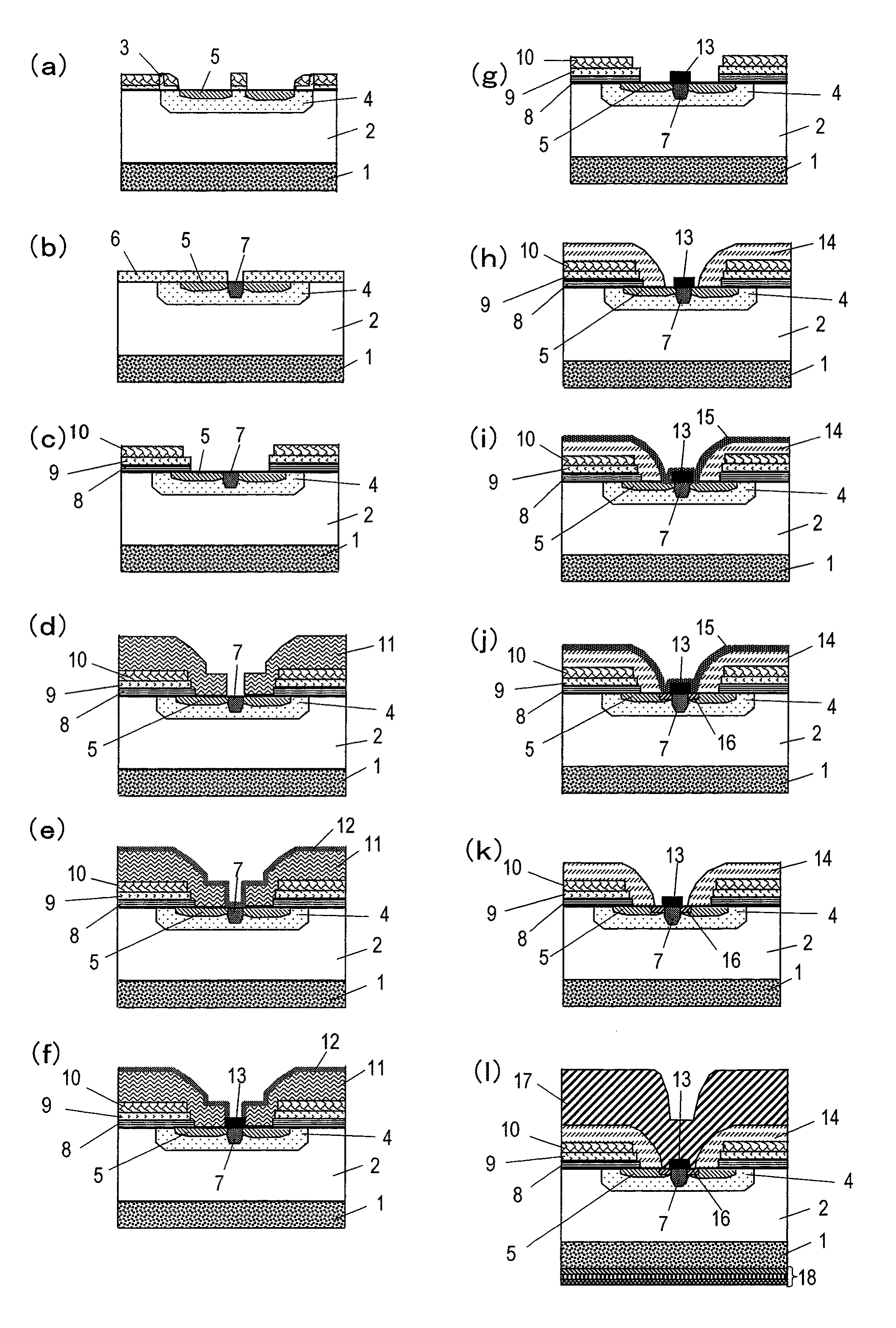
[0081]FIG. 3(a) is a schematic cross-sectional view showing a semiconductor device in Embodiment 1 According to the present invention. The semiconductor device shown in FIG. 3(a) includes a silicon carbide semiconductor layer 2.

[0082]The silicon carbide semiconductor layer 2 is formed of a silicon carbide semiconductor. The silicon carbide semiconductor layer 2 may be a bulk forming a semiconductor substrate or an epitaxial layer formed on a semiconductor substrate. In this embodiment, the silicon carbide semiconductor layer 2 is formed on a silicon carbide semiconductor substrate 1 by epitaxial growth. The silicon carbide semiconductor substrate 1 is an off substrate having an off angle of, for example, 8 degrees from the (0001) surface of 4H—SiC. The silicon carbide semiconductor substrate 1 is doped with an n-type impurity such as nitrogen, phosphorus, arsenic or the like at a concentration of, for example, 1×1018 cm−3 or higher, and has a low resistance. The silicon carbide semi...

embodiment 2

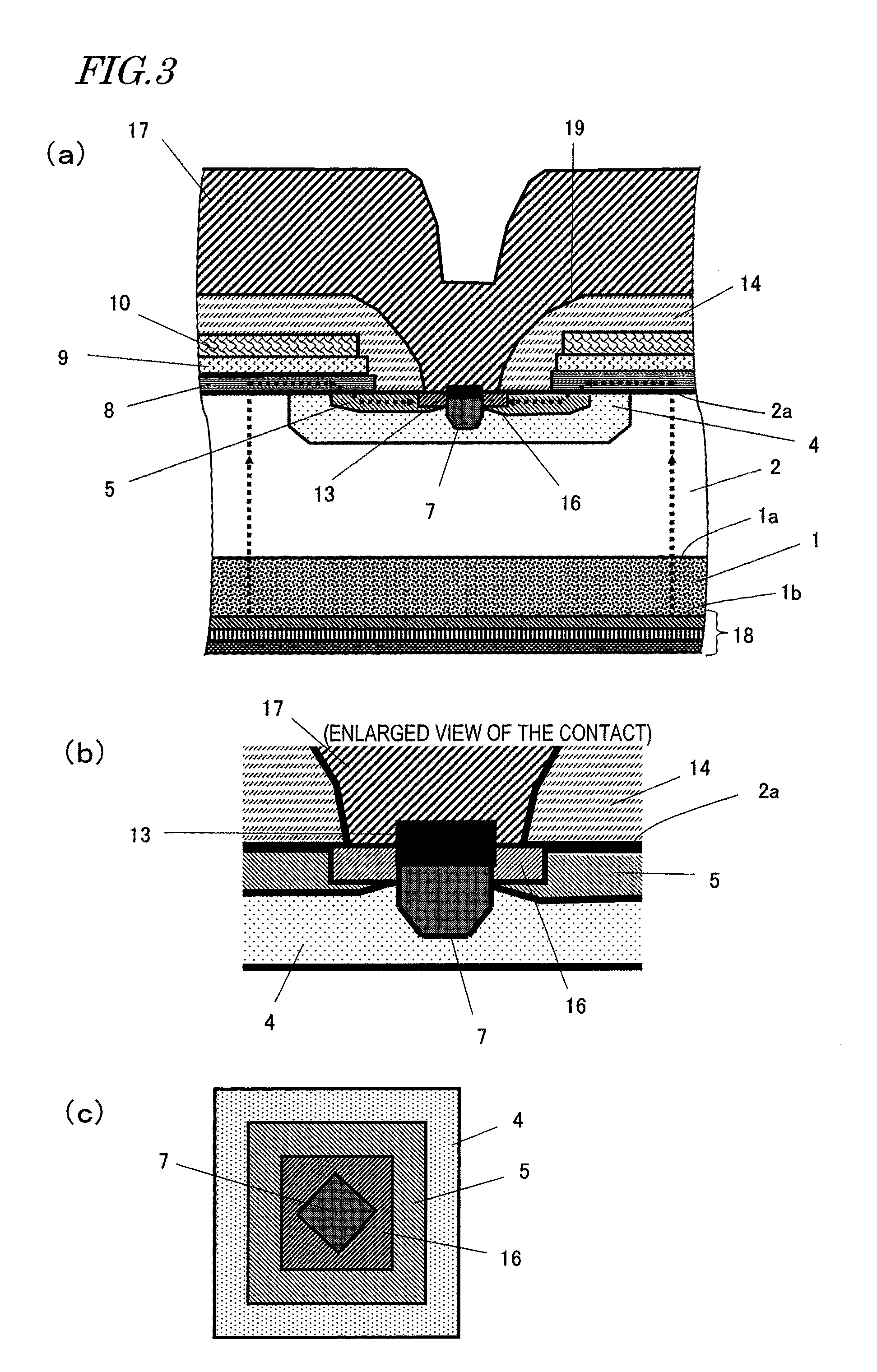
[0134]FIG. 5(a) is a schematic cross-sectional view showing a semiconductor device in Embodiment 2 according to the present invention. FIG. 5(b) is a cross-sectional view showing, in enlargement, a structure of an n-type ohmic electrode 16, a p-type ohmic electrode 13 and the vicinity thereof.

[0135]The semiconductor device in this embodiment is different from that in Embodiment 1 in the following points: (1) a nitrogenized titanium layer 15′ is provided on a side surface of the contact hole of the second interlayer insulating layer 14; (2) the n-type ohmic electrode 16 includes an n-type reaction layer 16a containing an alloy of titanium, silicon and carbon and a titanium nitride layer 16b; and (3) the p-type ohmic electrode 13 includes a p-type reaction layer 13a containing an alloy of nickel, aluminum, titanium, silicon and carbon and a titanium nitride layer 13b.

[0136]The nitrogenized titanium layer 15′, the titanium nitride layer 16b and the titanium nitride layer 13b are deriv...

experiment examples

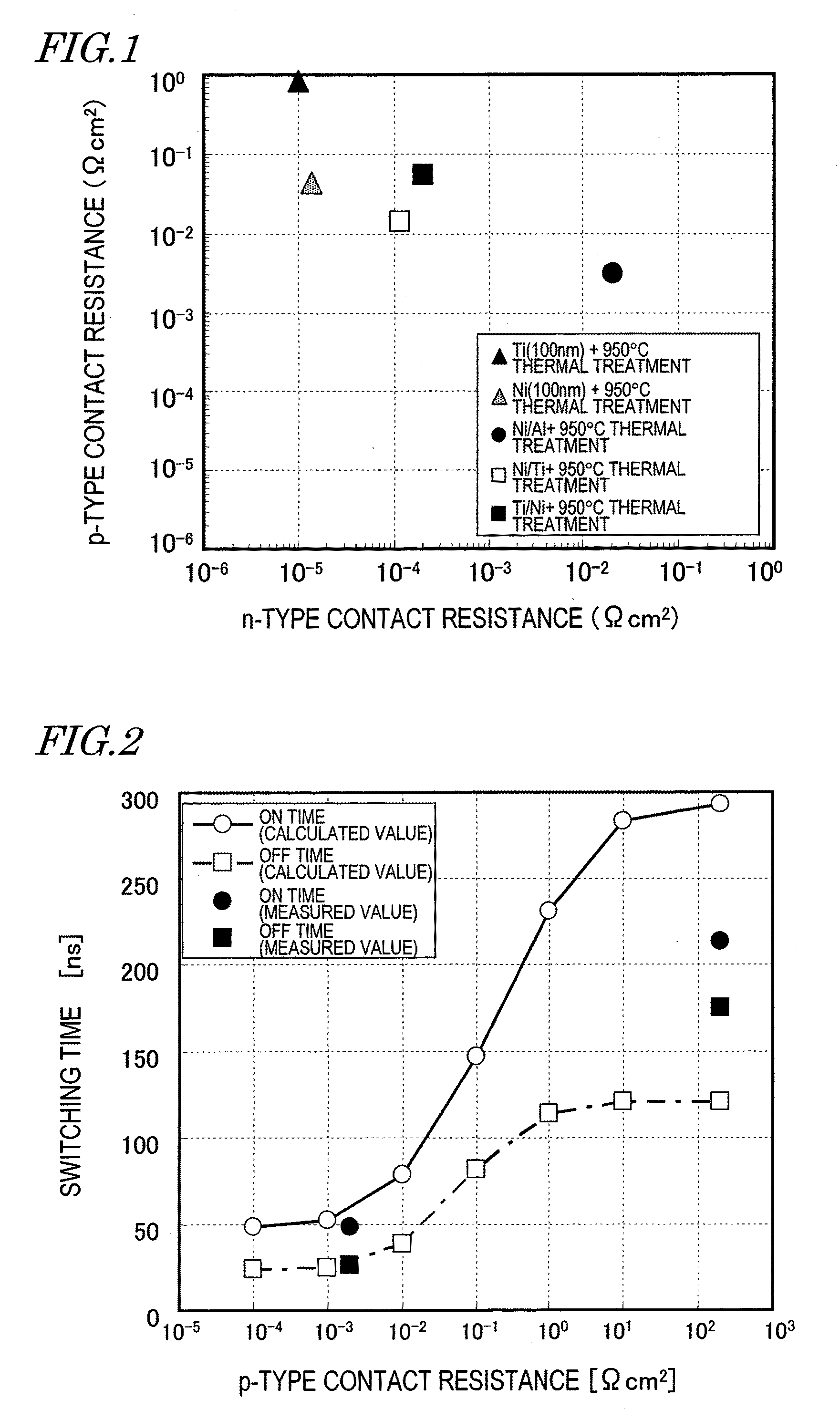
[0155]In order to confirm the effects of the present invention, the electric characteristics of the p-type ohmic electrode 13 were measured and the composition thereof was analyzed. The results are shown below.

1. Electric Characteristics of the P-Type Ohmic Electrode 13

[0156]FIG. 8 shows the current vs. voltage characteristic of a p-type contact formed as follows as in Embodiment 1. On a p-type silicon carbide semiconductor substrate having an impurity concentration of 5×1019 cm−3, a nickel / aluminum stacking layer, a nickel layer, and a titanium layer were each vapor-deposited and thermally treated at 950° C. for 2 minutes. As shown in FIG. 8, the ohmic characteristic provided by a nickel / aluminum layer shows a significant improvement in the current vs. voltage characteristic over the case where a silicide layer of a single nickel layer or a silicide layer of a single titanium layer is formed, and an ohmic characteristic is realized even at a low concentration of nickel / aluminum. Fr...


PUM

PropertyMeasurementUnit
temperatureaaaaaaaaaa

Abstract

A semiconductor device according to the present invention includes a silicon carbide semiconductor substrate having a silicon carbide semiconductor layer; a p-type impurity region provided in the silicon carbide semiconductor layer and including a p-type impurity; a p-type ohmic electrode electrically connected to the p-type impurity region; an n-type impurity region provided in the silicon carbide semiconductor layer adjacent to the p-type impurity region, and including an n-type impurity; and an n-type ohmic electrode electrically connected to the n-type impurity region. The p-type ohmic electrode contains an alloy of nickel, aluminum, silicon and carbon, and the n-type ohmic electrode contains an alloy of titanium, silicon and carbon.

Description

TECHNICAL FIELD[0001]The present invention relates to a silicon carbide semiconductor device, and in particular to a silicon carbide semiconductor device having n-type and p-type ohmic electrodes and a method for producing the same.BACKGROUND ART[0002]Conventionally, power devices using silicon (Si) semiconductors have been used as devices for power electronics. Devices for power electronics are required to operate at a higher frequency with a larger current. Various studies for research and development have been made to improve the performance of silicon power devices.[0003]However, the performance of the silicon power devices is now approaching the theoretical limit thereof. In addition, power devices are occasionally required to operate in severe environments, for example, at a high temperature or under radiation. Silicon semiconductors are not suitable to use in such severe environments. For these reasons, studies are being made regarding devices using semiconductor materials ot...

Claims


Application Information

Patent Timeline
Patent Type & Authority Patents(United States)
IPC IPC(8): H01L21/28H01L29/12H01L29/78
CPCH01L29/45H01L29/66068H01L29/7802H01L21/0485H01L29/086H01L29/1608Y10S438/931H01L29/7828
Inventor HAYASHI, MASASHIUTSUNOMIYA, KAZUYAKUSUMOTO, OSAMU
Owner PANASONIC CORP
Why Eureka
Try Eureka