
Control circuit of semiconductor device having over-heat protecting function

a technology of control circuit and semiconductor device, which is applied in the direction of incandescent lamp energy saving, pulse technique, sustainable buildings, etc., can solve the problems of deterioration of mosfet b>3/b>i>a /i>, possible deterioration of mosfet, and complicated circuit. and enlarged

Active Publication Date: 2010-08-03
YAZAKI CORP
View PDF5 Cites 3 Cited by
  • Summary
  • Abstract
  • Description
  • Claims
  • Application Information

AI Technical Summary

Benefits of technology

[0020]The present invention is devised by considering the above-described circumstances and it is an object to provide a control circuit of a semiconductor device having an over-heat protecting function that can solve the above-described problems.
[0034]According to the control circuit of the semiconductor device having the over-heat protecting function of the present invention, when the temperature detecting circuit of the over-heat protecting unit operates to turn on the gate interrupting circuit, then, the protecting operation is carried out by interrupting the gate of the semiconductor element and the control unit does not supply the PWM signal, the supply of the driving electric power by the driving electric power supply unit is continuously carried out only for a prescribed period by the timer unit. Accordingly, since the structure that the output state of the semiconductor element is fetched to decide whether or not the protecting operation is carried out to stop the PWM control of the semiconductor element is not required as usual, the circuit can be simplified and made to be compact.
[0035]Further, according to the control circuit of the semiconductor device having the over-heat protecting function of the present invention, when the temperature detecting circuit of the over-heat protecting unit operates to turn on the gate interrupting circuit, and then, the protecting operation is carried out by interrupting the gate of the semiconductor element, the supply of the driving electric power by the driving electric power supply unit is continuously carried out only for a prescribed period by the timer unit. Accordingly, the interruption of the gate by the gate interrupting circuit of the over-heat protecting unit is maintained, and the operations of several times are not required as usual for turning on again and over-heat interrupting the semiconductor element, so that the deterioration of the semiconductor element can be prevented.
[0036]Further, according to the control circuit of the semiconductor device having the over-heat protecting function of the present invention, when the temperature detecting circuit of the over-heat protecting unit operates to turn on the gate interrupting circuit, and then, the protecting operation is carried out by interrupting the gate of the semiconductor element, the supply of the driving electric power by the driving electric power supply unit is continuously carried out only for a prescribed period by the timer unit to maintain the interruption of the gate by the gate interrupting circuit of the over-heat protecting unit. Accordingly, when the interruption of the gate is maintained, even if a change arises in the PWM signal from the control unit, the semiconductor element is not turned on. Thus, a situation can be prevented that while the temperature of the semiconductor element is high, the semiconductor element is turned on again and then broken.

Problems solved by technology

Therefore, a problem arises that a circuit is complicated and enlarged.
Further, when it is decided whether or not the protecting operation is carried out, an operation that the MOSFET 3a is turned on again to be over-heat interrupted needs to be repeated several times. Thus, a problem also arises that the deterioration of the MOSFET 3a may possibly advance.
Thus, a problem arises that the MOSFET 3a may be possibly broken.

Method used


Image

  • Control circuit of semiconductor device having over-heat protecting function
  • Control circuit of semiconductor device having over-heat protecting function
  • Control circuit of semiconductor device having over-heat protecting function

Examples


embodiment

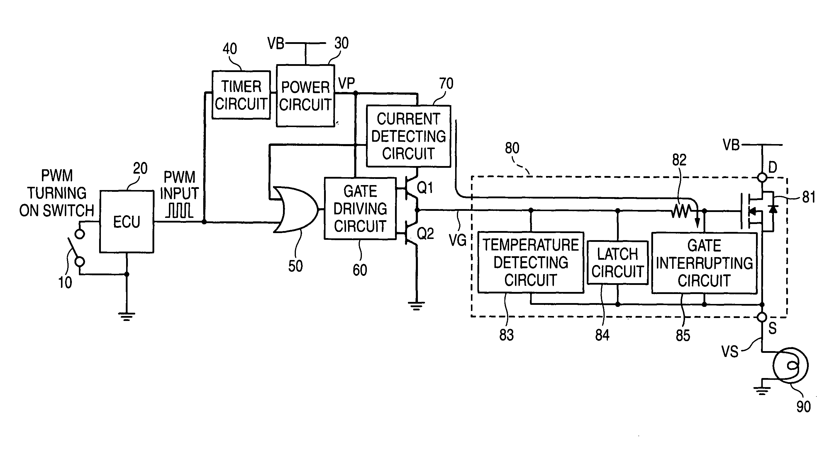
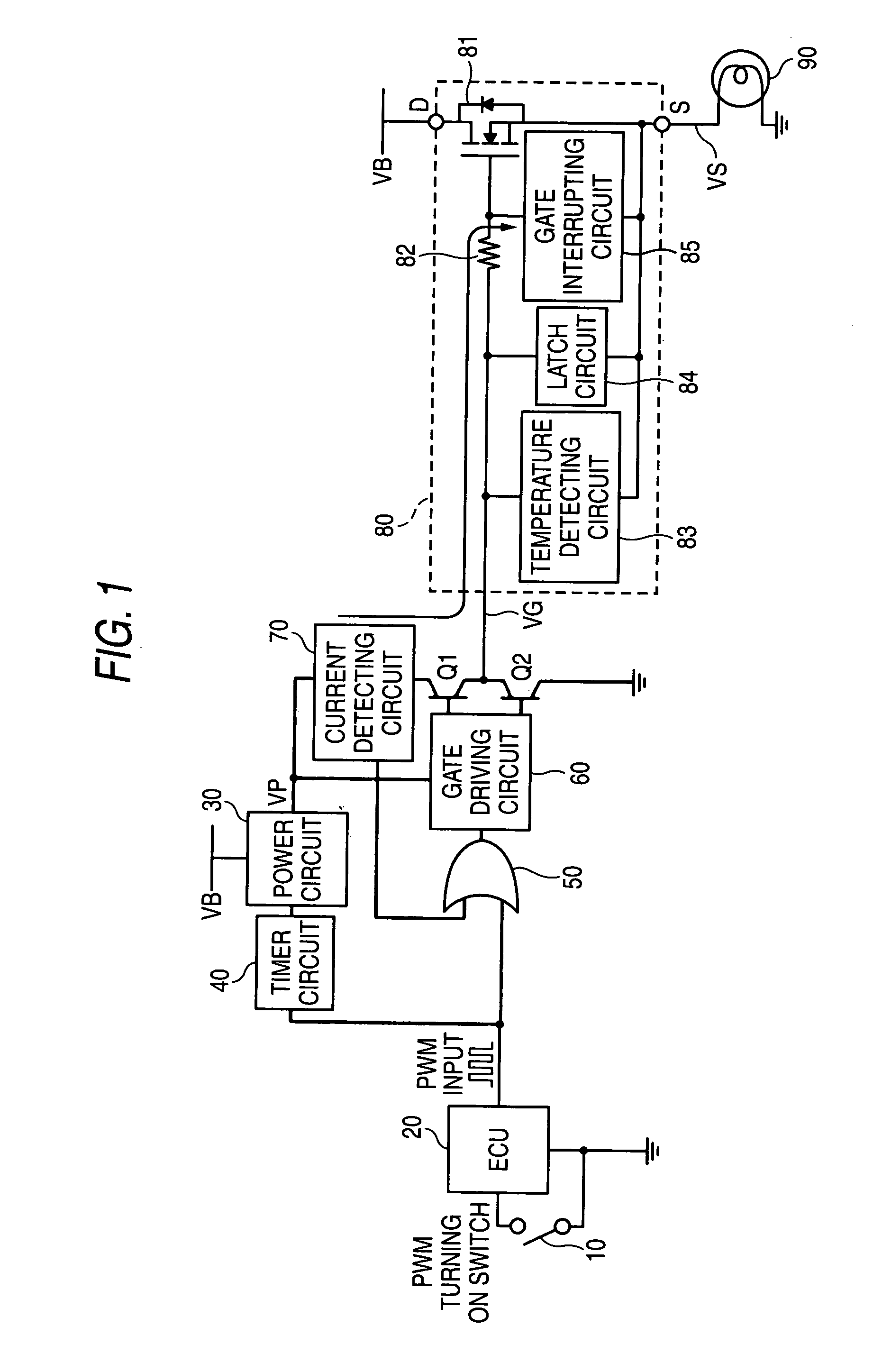
[0051]Now, embodiments of the present invention will be described below in detail. FIG. 1 is a diagram for explaining one embodiment of a control circuit of a semiconductor device having an over-heat protecting function according to the present invention.

[0052]The control circuit of the semiconductor device having the over-heat protecting function shown in FIG. 1 includes an ECU (Engine Control Unit) 20, a power circuit 30, a timer circuit 40, an OR gate 50, a gate driving circuit 60 and a current detecting circuit 70.

[0053]In the drawing, reference numeral 10 designates a PWM turning on switch and 90 designates, for instance a hazard lamp driven not only when an ignition switch is turned on, but also when the ignition switch is turned off. Reference numeral 80 designates the semiconductor device having the over-heat protecting function.

[0054]The ECU outputs a PWM (Pulse Width Modulation) signal with a predetermined duty ratio in accordance with an operation of the PWM turning on sw...


PUM


Abstract

A control circuit of a semiconductor device includes: a semiconductor element which supplies an electric power to a load; an over-heat protecting unit having: a temperature detecting section which detects a rise in temperature; a latch section which holds an output of the temperature detecting section; and a gate interrupting section which interrupts an input to a gate of the semiconductor element in accordance with the output of the latch section; a control unit which supplies a PWM signal for turning on / off the semiconductor element; a driving electric power supply unit which supplies a driving electric power for driving the over-heat protecting unit; and a timer unit which allows the driving electric power supply unit to supply the driving electric power for a predetermined period when the input to the gate of the semiconductor element is interrupted and the control unit stops to supply the PWM signal.

Description

BACKGROUND OF THE INVENTION[0001]1. Technical Field[0002]The present invention relates to a control circuit of a semiconductor device having an over-heat protecting function suitable for preventing, due to an over-heat, a damage of a semiconductor element for a large electric power used for driving, for instance, a lamp of a motor vehicle.[0003]2. Background Art[0004]As the control circuit of a semiconductor device having an over-heat protecting function, JP-B-3585105 discloses a device that can reduce a possibility of breaking the semiconductor device. This device includes, as shown in FIG. 6, a CPU 1, an amplifying circuit 2, a semiconductor device 3 having an over-heat protecting function for turning on / off a driving of a load 4 and an output state detecting part 5.[0005]The CPU 1 internally generates (or fetches from an external signal source not shown in the drawing) a control signal for controlling the semiconductor device 3 having the over-heat protecting function, for instan...

Claims


Application Information

Patent Timeline
Patent Type & Authority Patents(United States)
IPC IPC(8): H02H5/04
CPCH03K17/08122H03K17/18H05B39/047H03K2017/0806H01L2924/0002Y02B20/144H01L2924/00Y02B20/00
Inventor YABE, HIROOKUBOTA, KAZUHIROSASAHARA, MASATO
Owner YAZAKI CORP
Learn More