AC/DC light emitting diodes with integrated protection mechanism
- Summary
- Abstract
- Description
- Claims
- Application Information
AI Technical Summary
Problems solved by technology
Method used
Image
Examples
first embodiment
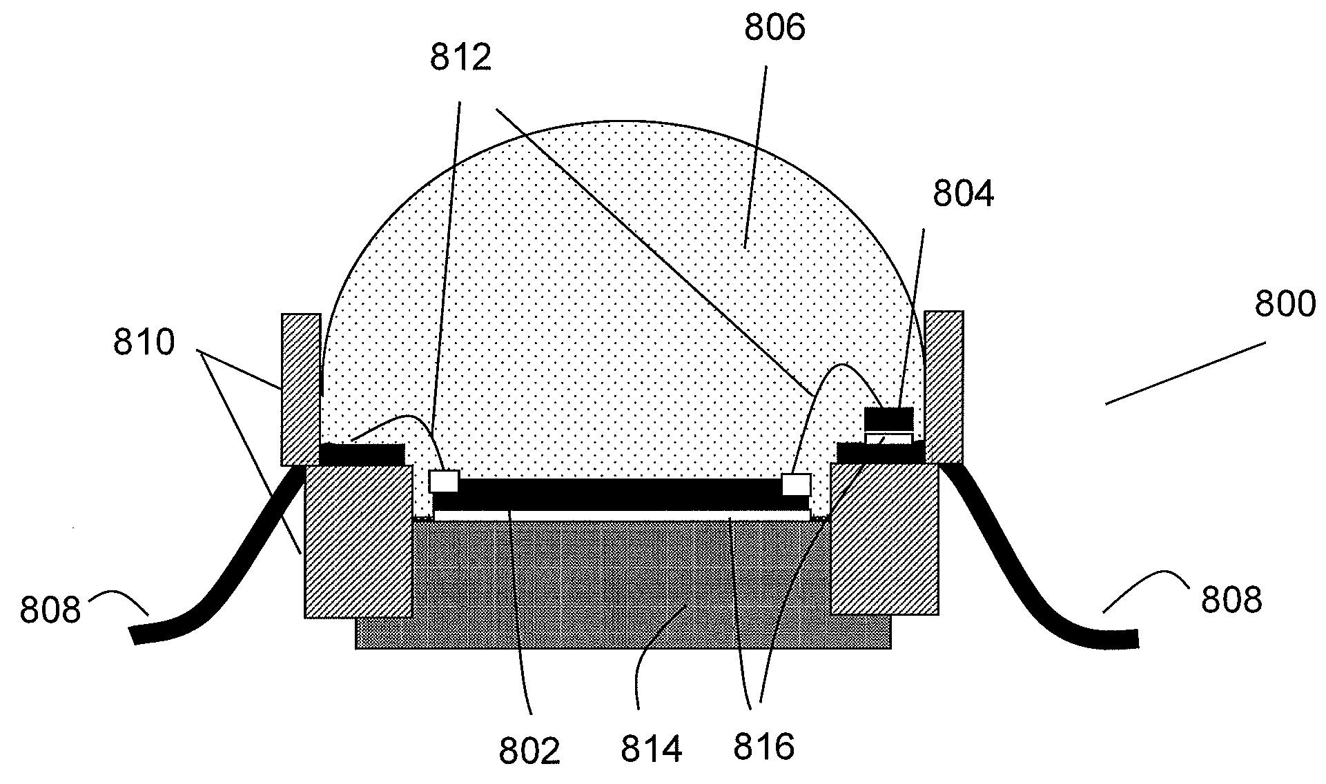
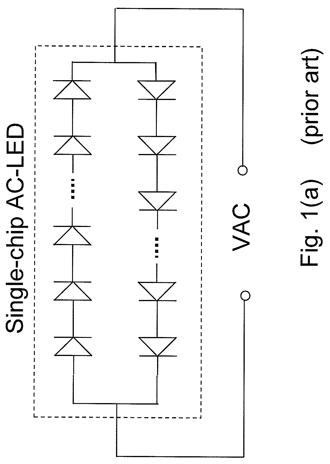
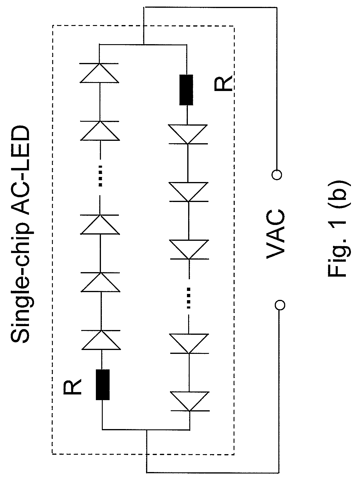
[0045]In a first embodiment, the doped n-type semiconductor material of LED is used to fabricate the resistor with a designed resistance value. Referring to FIG. 3(a), the wafer is first etched to n-GaN layer 13 to expose doped n-GaN, and then etched to insulating substrate 11 to isolate each individual LED. Current spreading layer 20, p-contact 19, and n-contact 18 are formed by metal deposition. Next, an insulation material 16 is deposed on the etched sidewall, and then metal line 17 is formed to serially connect individual mini-LEDs (micro-LEDs) to form one AC-LED. To monolithically integrate the current-limiting resistor by using doped n-GaN layer 13, during the first etching step down to the doped n-GaN layer 13, the etching depth is controlled so that about 0.5-2 μm doped n-GaN layer 13 remains. In the second etching step down to the insulating substrate, n-GaN strip with certain geometry is formed. After two n-contacts 18 deposited on the two ends of GaN strip, one end is con...
embodiment 900
[0060]In another embodiment 900 disclosed in FIG. 9, an AC-LED chip 906 is flip-chip mounted on a submount 902 (see the description for FIG. 3(b) which discusses how this can be done), and the protection circuits and elements are then integrated onto that same submount 902. This arrangement enables the incorporation of more complex protection. For example, a varistor 908 can be integrated on the submount such that it is connected across the AC power input. Thus, when a power surge or voltage spike is sensed, the varistor's resistance rapidly decreases, creating an instant shunt path and protecting the AC-LED itself. In the disclosed preferred embodiment, metal oxide varistors (MOV) are preferred. But other devices could also be incorporated to accomplish the same objectives and still fall within the scope of the present invention.
[0061]Other arrangements could also be incorporated into the already described physical arrangements. For example, in FIG. 9, 904 is a tiny surface mounted...
PUM
 Abstract
Description
Claims
Application Information
 - R&D
- Intellectual Property
- Life Sciences
- Materials
- Tech Scout
- Unparalleled Data Quality
- Higher Quality Content
- 60% Fewer Hallucinations
Browse by: Latest US Patents, China's latest patents, Technical Efficacy Thesaurus, Application Domain, Technology Topic, Popular Technical Reports.
© 2025 PatSnap. All rights reserved.Legal|Privacy policy|Modern Slavery Act Transparency Statement|Sitemap|About US| Contact US: help@patsnap.com


