
Liquid crystal device and electronic apparatus

a liquid crystal device and electronic equipment technology, applied in non-linear optics, instruments, optics, etc., can solve the problems of likely to have a contact failure, and inability to ensure electrical reliability, so as to achieve high anti-corrosion, high anti-corrosion, and simple connection

Active Publication Date: 2010-03-02
JAPAN DISPLAY WEST
View PDF35 Cites 13 Cited by
  • Summary
  • Abstract
  • Description
  • Claims
  • Application Information

AI Technical Summary

Benefits of technology

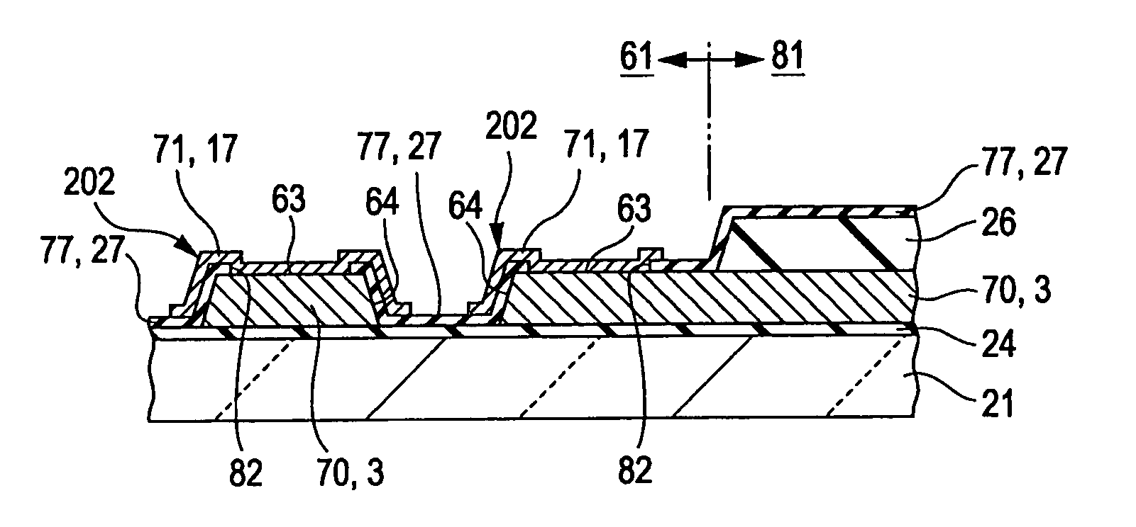
[0010]With this configuration, in an FFS mode liquid crystal device having a planarizing film, because the electrode insulating film provided between the first electrode and the second electrode is arranged in the terminal region (the region in which the planarizing film is not formed) as the terminal insulating film, the terminal insulating film serves as a passivation film for the terminal. In addition, because the connection between the mounting component and the terminal is formed of one layer of the terminal electrode portion, it is possible to ensure a larger area of the connection. Furthermore, because the terminal body portion is made of the same material as that of the signal wiring, they may be formed at the same time, and it is possible to simplify a connection between the terminal and the signal wiring. In the terminal region, when the planarizing film is left, it is necessary to form a through-hole having a few micrometers in the planarizing film. Thus, it is very likely to have a contact failure when connection is made to an electrode located at the bottom of the deep through-hole. Moreover, when the electrode of the terminal is formed using a conductive film for forming the first electrode and the second electrode, there is a possibility that, when the through-hole is deep, it is impossible to ensure electrical reliability due to poor adhesion. In the above configuration, in the terminal region, because the electrode is provided in the region in which the planarizing film is not formed, unevenness of the terminal region is reduced, and it is possible to ensure good conduction at the connection. In addition, because the side face of the terminal body portion is covered with the terminal insulating film and the terminal electrode portion, it is possible to ensure high anti-corrosion.
[0022]In addition, the liquid crystal device according to the aspects of the invention may be configured so that the mounting component is connected through the terminal. Furthermore, a sixth aspect of the invention provides an electronic apparatus having the liquid crystal device according to the above aspects of the invention. Thus, it is possible to achieve an electronic apparatus that is provided with a liquid crystal display portion of a terminal structure having high anti-corrosion and good electrical conduction.

Problems solved by technology

Thus, it is very likely to have a contact failure when connection is made to an electrode located at the bottom of the deep through-hole.
Moreover, when the electrode of the terminal is formed using a conductive film for forming the first electrode and the second electrode, there is a possibility that, when the through-hole is deep, it is impossible to ensure electrical reliability due to poor adhesion.

Method used


Image

  • Liquid crystal device and electronic apparatus
  • Liquid crystal device and electronic apparatus
  • Liquid crystal device and electronic apparatus

Examples


first embodiment

[0060]A liquid crystal device according to a first embodiment of the invention will now be described with reference to FIG. 1 to FIG. 5I. The liquid crystal device according to the first embodiment is of an active matrix type that uses an LTPS (low-temperature polysilicon) TFT element as a pixel switching element. The liquid crystal device is an example of an FFS mode transmissive liquid crystal device.

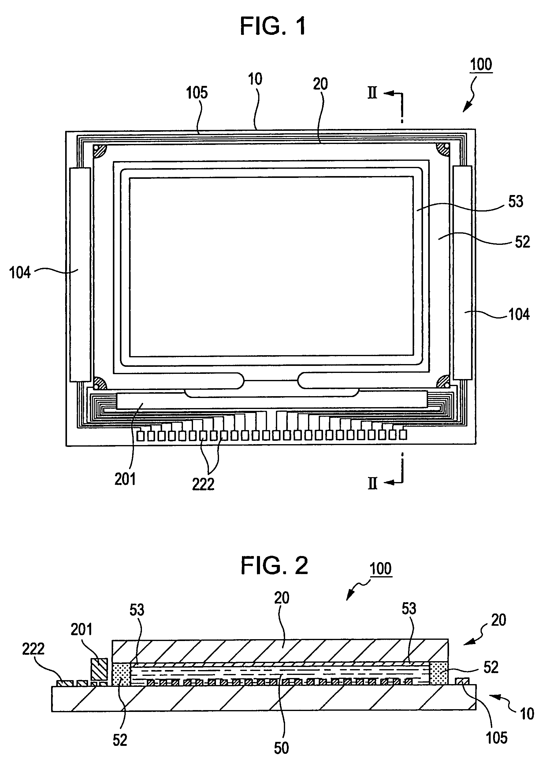
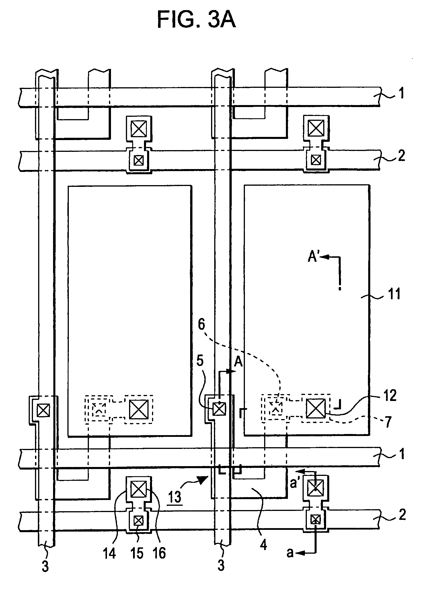
[0061]FIG. 1 is a plan view of a liquid crystal device with component elements according to the present embodiment as viewed from the side of an opposite substrate. FIG. 2 is a cross-sectional view that is taken along the line II-II in FIG. 1. FIG. 3A and FIG. 3B are enlarged plan views of pixels on an element substrate of the liquid crystal device. FIG. 4 is a cross-sectional view of the liquid crystal device, taken along the line A-A′ and line a-a′ in FIG. 3A or FIG. 3B. FIG. 5A to FIG. 5I are cross-sectional views showing a process of manufacturing the liquid crystal device. Note t...

second embodiment

[0089]A liquid crystal device according to a second embodiment of the invention will now be described. Note that, in the liquid crystal device according to the second embodiment and other following embodiments, the configurations in the display areas are the same as that of the first embodiment but the terminals 202 formed in the region outside the display area differ from those of the first embodiment. Therefore, the liquid crystal devices according to the second embodiment and the other following embodiments will be described by focusing on a process of manufacturing the terminals 202 and the structure thereof. The liquid crystal device according to the second embodiment, in short, has a configuration that the terminal body portions 70 and the side portions 64 are covered with an ITO film formed in the same layer of the pixel electrodes together with the terminal insulating film 77 and the terminal electrode portions 71 formed in the same layer of the common electrode. That is, in...

third embodiment

[0095]A liquid crystal device according to a third embodiment of the invention will now be described. The liquid crystal device according to the third embodiment, in short, is configured so that the lower layer terminal electrode portions 72 that cover the terminal body portions 70 in the second embodiment are removed at the terminal connections 63 and left at the side portions 64. That is, in the third embodiment, the side portions 64 are covered with two layers of ITO film, and the terminal connections 63 are covered with one layer of ITO film.

[0096]FIG. 13A to FIG. 13F are cross-sectional views, taken along the line VII-VII in FIG. 6, showing a process of manufacturing the region 61 in the TFT array substrate 10 of the liquid crystal device according to the third embodiment. FIG. 13A is the same as the first process shown in FIG. 9A according to the first embodiment. FIG. 13B is also the same as the second process shown in FIG. 9B. In the third embodiment, after the wirings 62 an...


PUM

PropertyMeasurementUnit
thicknessaaaaaaaaaa
thicknessaaaaaaaaaa
thicknessaaaaaaaaaa

Abstract

A liquid crystal device includes a first substrate, a second substrate, liquid crystal, a switching element, a signal wiring, a planarizing film, a first electrode, an electrode insulating film, a second electrode, and a terminal. The terminal is provided at least in a portion of a region on the first substrate in which the planarizing film is not formed. The terminal includes a terminal body portion, a terminal insulating film, and a terminal electrode portion. The terminal body portion is made of the same material as that of the signal wiring. The terminal insulating film is made of the same material as that of the electrode insulating film. The terminal electrode portion is made of the same material as that of the second electrode. The terminal electrode portion is electrically connected to the terminal body portion through the opening region.

Description

BACKGROUND[0001]1. Technical Field[0002]The present invention relates to a liquid crystal device and an electronic apparatus.[0003]2. Related Art[0004]An existing TN (twisted nematic) liquid crystal device has a configuration such that liquid crystal is sealed between a pair of substrates, and an electric field is applied in a direction perpendicular to the surfaces of the substrates by means of electrodes formed on the substrates to control alignment of liquid crystal molecules and thereby modulates light transmittance ratio. In contrast, one type of liquid crystal device that attempts to increase the viewing angle is known, in which the direction in which an electric field is applied to liquid crystal is set in a direction substantially parallel to the surface of the substrate and the liquid crystal is rotated within a plane that is substantially parallel to the substrate using the electric field. In other words, this mode is configured so that a pair of electrodes are formed on o...

Claims


Application Information

Patent Timeline
Patent Type & Authority Patents(United States)
IPC IPC(8): G02F1/1345
CPCG02F1/1345G02F1/13452G02F1/134363G02F2001/133388G02F2001/134372G02F2001/13456G02F1/133388G02F1/13456G02F1/134372G02F1/1343
Inventor FUJITA, SHIN
Owner JAPAN DISPLAY WEST
Learn More