
Organic species that facilitate charge transfer to or from nanostructures

a charge transfer and organic species technology, applied in the field of nanotechnology, can solve the problems of polymerization and inability to make optimal contact with nanocrystals, and the general limitation of charge transport within photovoltaic devices

Active Publication Date: 2009-08-11
SHOEI CHEM IND CO LTD
View PDF35 Cites 122 Cited by
  • Summary
  • Abstract
  • Description
  • Claims
  • Application Information

AI Technical Summary

Benefits of technology

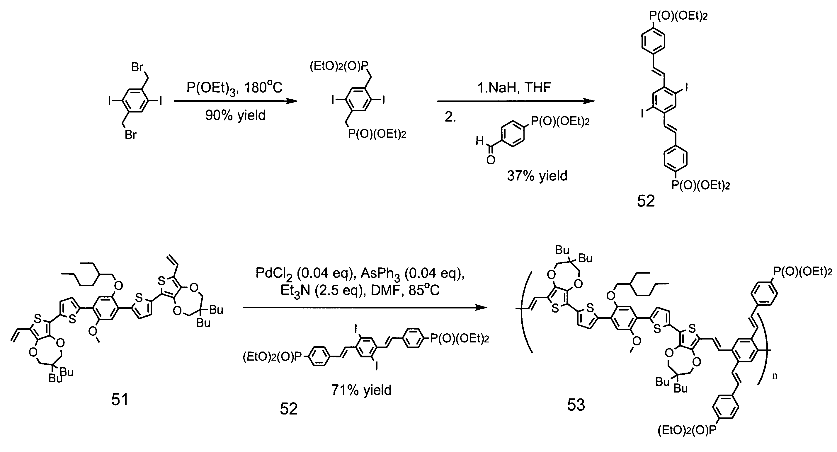
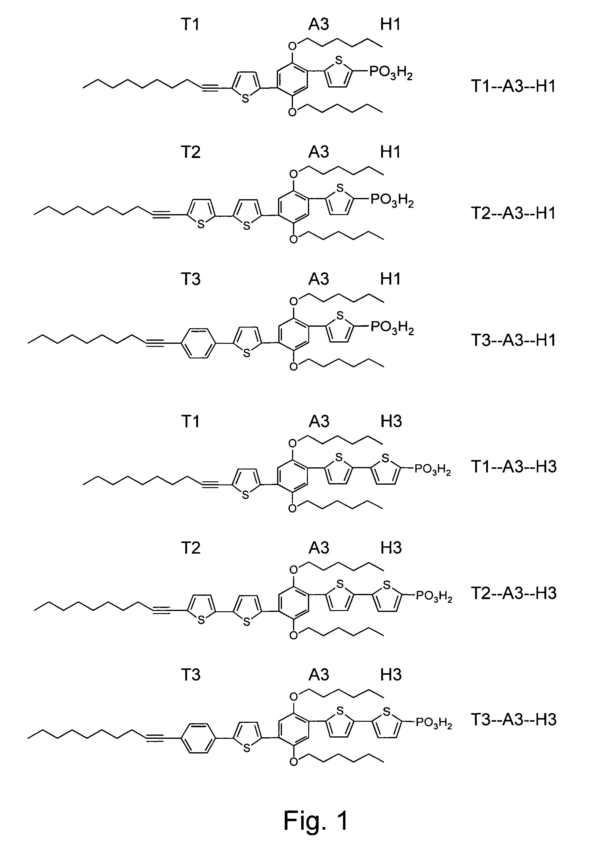
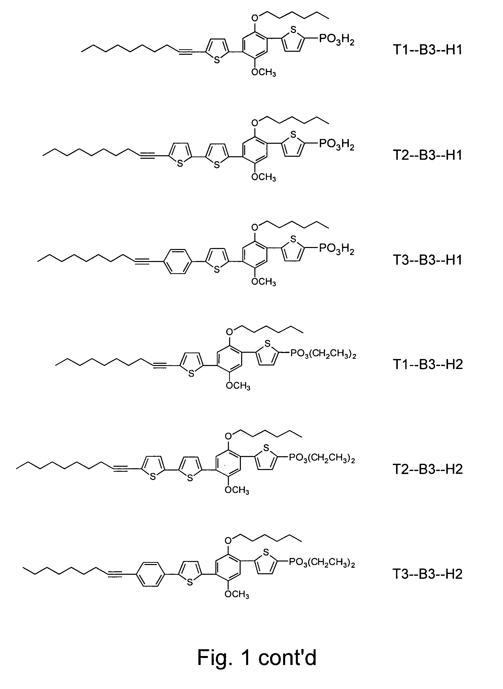
[0009]In one aspect, the present invention provides conductive compositions for modification of charge transport across a nanostructure (e.g., nanocrystal)-containing matrix. The conductive composition typically include a) a conjugated organic moiety as the “body structure,” or core of the conductive molecule; b) a nanostructure (e.g., nanocrystal)-binding “head group” coupled to the body structure at a first position on the conjugated organic moiety; and c) a “tail group” coupled to the body structure at a second position on the conjugated organic moiety. After formation of an exciton in the nanostructure-containing matrix, the conductive composition facilitates the injection and / or extraction of charge (electron and / or hole) with respect to the attached nanostructure, thereby modifying charge transport across a nanostructure-containing matrix.
[0023]At least one substituent of the first, second or third substituent modules is capable of binding to a nanostructure surface (or, optionally, the component is already bound to a nanostructure surface). Coupling of the various modules to the body structure does not destroy the electronic conjugation of the body structure. Rather, in a preferred embodiment, coupling of one or more of the substituent modules to the body structure extends the conjugation of the body structure.

Problems solved by technology

However, charge transport within the photovoltaic device is generally limited by matrix constraints, rather than by the absorption properties of the nanocrystals.
As such, these polymers do not make optimal contact with the nanocrystal.

Method used


Image

  • Organic species that facilitate charge transfer to or from nanostructures
  • Organic species that facilitate charge transfer to or from nanostructures
  • Organic species that facilitate charge transfer to or from nanostructures

Examples


example 1

Synthesis of Model Conductive Composition 4-Decynyl-Benzene-1-Phosphonic Acid

[0170]A synthesis protocol was designed to test the modular approach to synthesis of the conductive compositions of the present invention (FIG. 3). The model conductive composition 5b was prepared using 1-iodo-4-bromobenzene as a precursor to the body structure, 1-decyne as the tail group moiety, and diethylphosphite as the head group moiety. To a 500 mL schlenk flask with egg-shaped stirbar under argon, palladium dichloride (1.0 mmol, 0.177 g), copper(I) iodide (2.36 mmol, 0.450 g), and triphenylphosphine (2.0 mmol, 0.525 g) were added in a glovebox under argon. On a schlenk line, 1-iodo-4-bromo-benzene (50 mmol, 14.15 g, compound 1) was added, the vessel was stoppered, and the flask was placed under vacuum and backfilled with argon (3×). The flask was fitted with a septum under positive argon pressure and degassed diisopropyl amine (100 mL) was added via cannula under positive argon pressure with stirring...

example 2

Synthesis of Conductive Composition 16

[0173]One advantage to the methods of the present invention is the modular approach to synthesis of the various conductive compositions of interest. Using this approach allows for the preparation and use of common synthetic intermediates and core structures. An exemplary synthesis scheme for the preparation of a conductive composition of the present invention is depicted in FIG. 4 and described in further detail herein. In this modular approach, the various components of the composition (body structure, head group, tail group) are synthesized as individual structures, which are then coupled together to form the conductive composition.

[0174]Preparation of the Head Group Precursor

[0175]One common intermediate in the synthesis of some embodiments of the present invention is the activated head group precursor compound 9, which can be prepared based upon known synthetic protocols such as those provided in FIG. 4.

[0176]Coupling of Sidearm Moieties to ...

example 3

Synthesis of Compositions Having Asymmetric Sidearm Elements

[0183]The two sidearm moieties of the conductive composition need not be identical or symmetrical in structure. In another embodiment of the compositions of the present invention, two differing sidearm moieties are employed in the modular synthesis of the conductive composition 21. As shown in FIG. 5, 4-methoxyphenol (compound 17) was alkylated at the unprotected hydroxyl group using 1.1 equivalents of 1-iodohexane (compound 11) in the presence of potassium carbonate and DMF at 70° C., to form intermediate compound 18 (see FIG. 15), which was iodinated (compound 19, FIG. 17), derivatized with thiophene moieties, and coupled to a 1-decyne tail moiety (Ti) and a thiophene-phosphonate head group (H3) in a manner similar to Example 2.


PUM

PropertyMeasurementUnit
aspect ratioaaaaaaaaaa

Abstract

The present invention provides polymeric compositions that can be used to modify charge transport across a nanocrystal surface or within a nanocrystal-containing matrix, as well as methods for making and using the novel compositions.

Description

CROSS-REFERENCE TO RELATED APPLICATIONS[0001]This application is a continuation-in-part of nonprovisional application U.S. Ser. No. 10 / 656,910 filed Sep. 4, 2003, now U.S. Pat. No. 6,949,206 which in turn is related to U.S. provisional applications U.S. Ser. No. 60 / 408,722, filed Sep. 5, 2002; and U.S. Ser. No. 60 / 452,232, filed Mar. 4, 2003. The present application claims priority to and benefit of each of these prior applications, which are hereby incorporated herein by reference in their entirety for all purposes.FIELD OF THE INVENTION[0002]The present invention is in the field of nanotechnology. More particularly, the present invention is directed to conductive ligands, polymers and matrices for use with nanostructures, as well as related methods for producing and using the conductive compositions, and related devices incorporating the conductive compositions.BACKGROUND OF THE INVENTION[0003]Polymer-based light-emitting and photovoltaic devices, including those incorporating nan...

Claims


Application Information

Patent Timeline
Patent Type & Authority Patents(United States)
IPC IPC(8): H01B1/12C09K11/00C09K11/08H01L31/00H01L51/00H01B1/00
CPCB82Y10/00B82Y15/00B82Y30/00G01N33/588H01L51/0068H01B1/128H01L51/4226H01G9/2031H01G9/2059H10K85/655H10K30/50H10K30/151
Inventor WHITEFORD, JEFFERY A.BURETEA, MIHAI A.NGUYEN, LINHSCHER, ERIK
Owner SHOEI CHEM IND CO LTD
Learn More