
Nonvolatile semiconductor memory device and method of operating the same which stably perform erase operation

a nonvolatile semiconductor and memory device technology, applied in static storage, digital storage, instruments, etc., can solve the problems of affecting the operation of erase-verify, so as to achieve appropriate and accurate control of threshold voltage variations, avoid erase-verify of memory cells on unselected word lines, and achieve the effect of avoiding erase-verify

Inactive Publication Date: 2009-06-16
RENESAS ELECTRONICS CORP
View PDF7 Cites 10 Cited by
  • Summary
  • Abstract
  • Description
  • Claims
  • Application Information

AI Technical Summary

Benefits of technology

The present invention provides a nonvolatile semiconductor memory device that can selectively erase memory cells while avoiding harmful effects on unselected cells. This is achieved by applying a negative voltage to the selected word line and a positive voltage to the unselected word lines during an erase operation. The voltage difference between the substrate voltage and the negative voltage of the selected word line is applied to the memory cells on the selected word line, while the voltage difference between the substrate voltage and the positive voltage of the unselected word lines is applied to the memory cells on the unselected word lines. This results in a smaller voltage difference applied to the memory cells on the unselected word lines, avoiding erasing of these cells. The invention allows for more accurate and appropriate control of threshold voltages at memory cells during erasing without harmful effects on unselected cells.

Problems solved by technology

However, it is expected with the miniaturization of memory cells that the variations in threshold voltages rise to a level that no longer can be ignored.
In that case, for example, there is a possibility that over-erasing is too spread to be coped with by the typical erase-verify operation.
Therefore, when an over-erased memory cell is caused in performing collective erasing to a sector, it is difficult at the time of erase-verify to correctly read data of the other memory cells that share the bit line with the over-erased memory cell.
As a result, it is difficult to correctly perform erase-verify.
As a result, the unselected word lines are susceptible to the effect of voltage noise, which may cause false operation.
However, when erasing is performed in units of a word line, there is a possibility that erasing is also caused to a memory cell on an unselected word line, which has been revealed by the inventors' study.
In this case, it is not possible to apply a high voltage to only one of the gate and the substrate (e.g. gate voltage is 10 V while substrate voltage is 0 V), considering withstand voltage and so forth of a device itself.
In this case, this related art does not make it possible to control variations in erasing distribution, where +5 V voltage is applied to erasing unselected cells.

Method used


Image

  • Nonvolatile semiconductor memory device and method of operating the same which stably perform erase operation
  • Nonvolatile semiconductor memory device and method of operating the same which stably perform erase operation
  • Nonvolatile semiconductor memory device and method of operating the same which stably perform erase operation

Examples


Embodiment Construction

[0029]The invention will be now described herein with reference to illustrative embodiments. Those skilled in the art will recognize that many alternative embodiments can be accomplished using the teachings of the present invention and that the invention is not limited to the embodiments illustrated for explanatory purposed.

[0030]Embodiments of a nonvolatile semiconductor memory device and a method of operating the nonvolatile semiconductor memory device according to the present invention will be described below with reference to the attached drawings.

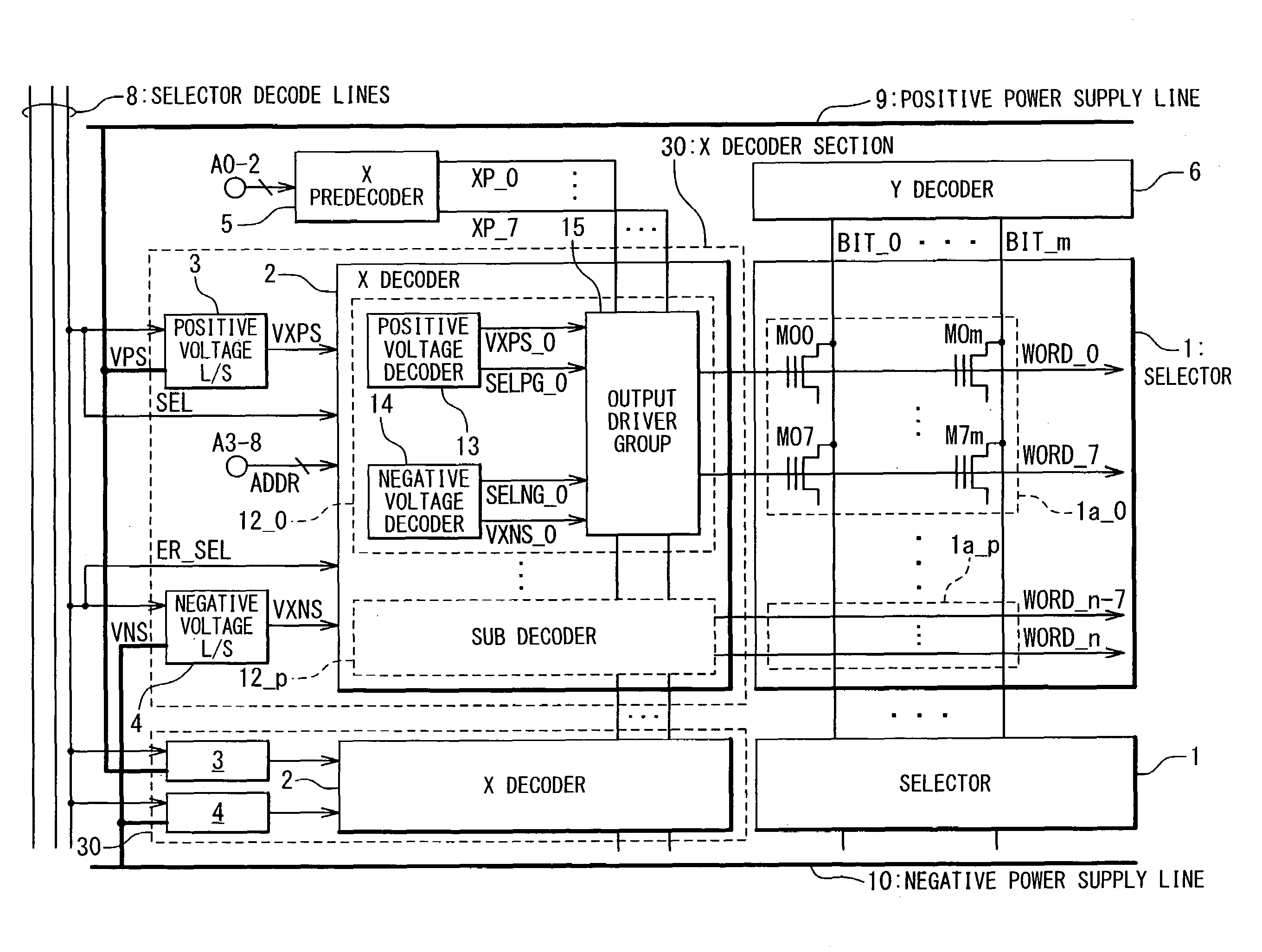
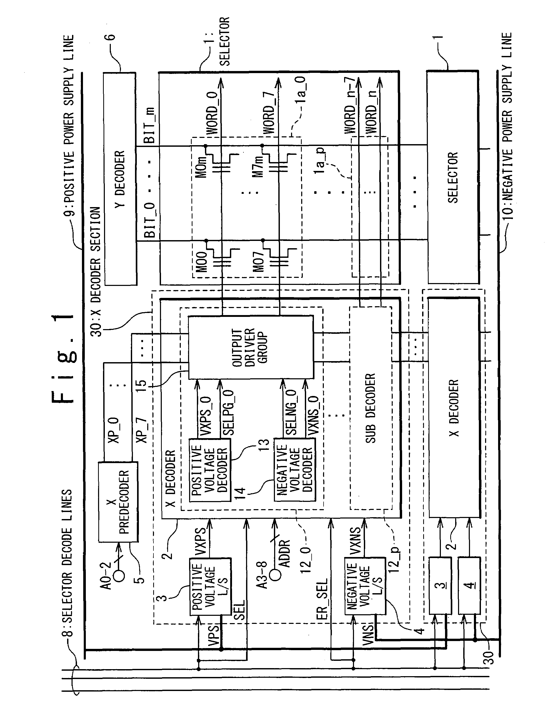
[0031]FIG. 1 is a block diagram showing a structure of a nonvolatile semiconductor memory device in an embodiment of the present invention. The nonvolatile semiconductor memory device 20 includes a plurality of sectors 1, a plurality of X-decoder sections 30, an X-predecoder 5, a Y-decoder 6, a plurality of sector decode lines 8, a positive power supply line 9, and a negative power supply line 10.

[0032]Each of the sectors 1 (memory cel...


PUM


Abstract

A nonvolatile semiconductor memory device includes a memory array and an X-decode section. The memory array includes a plurality of nonvolatile memory cells arranged in a matrix form and a plurality of word lines. The X-decode section selects a selected word line selected from the plurality of word lines, supplies a negative voltage to the selected word line, and supplies a positive voltage to unselected word lines which are not the selected word line, at the time of an erase operation.

Description

BACKGROUND OF THE INVENTION[0001]1. Field of the Invention[0002]The present invention relates to a nonvolatile semiconductor memory device and a method of operating the nonvolatile semiconductor memory device.[0003]2. Description of Related Art[0004]Nonvolatile semiconductor memory devices, such as flash memories, have been known which perform nonvolatile storage of data. In general, the flash memories perform an erase operation collectively in units of a sector or memory cell array. That is to say, erasing is performed at the erase operation by supplying negative voltage to gates of all memory cells after writing (programming) is performed to those memory cells in a sector to be erased. At this time, there are variations in threshold voltages at the memory cells after the erasing, due to variations in the properties of the memory cells in the sector. For this reason, it is possible that there is a memory cell where over-erasing is caused among the memory cells in the sector. To cop...

Claims


Application Information

Patent Timeline
Patent Type & Authority Patents(United States)
IPC IPC(8): G11C16/06
CPCG11C16/16G11C16/344G11C16/3445G11C16/3477
Inventor WATANABE, KAZUOSUGAWARA, HIROSHI
Owner RENESAS ELECTRONICS CORP
Learn More