
Method and apparatus for performing computations using residue arithmetic

a technology of residue arithmetic and computation method, applied in computation using denominational number representation, instruments, computing, etc., can solve the problems of inability to fully understand the speed, area and power characteristics of prior computation techniques using rns, and the inability to implement large-scale digital signal processors using a single semiconductor device. , the effect of reducing the size or power

Inactive Publication Date: 2009-04-21
THE ATHENA GROUP
View PDF19 Cites 11 Cited by
  • Summary
  • Abstract
  • Description
  • Claims
  • Application Information

AI Technical Summary

Benefits of technology

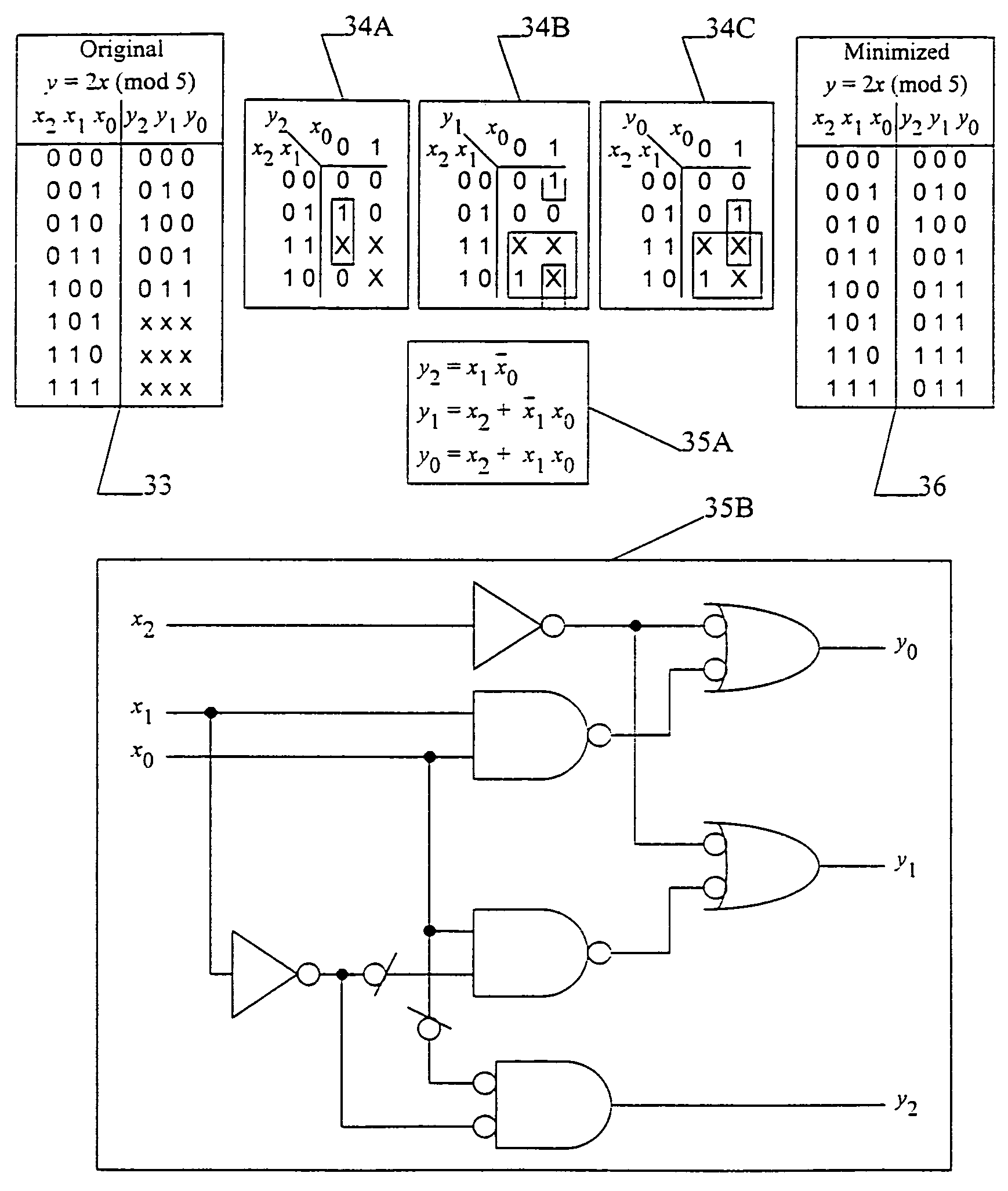
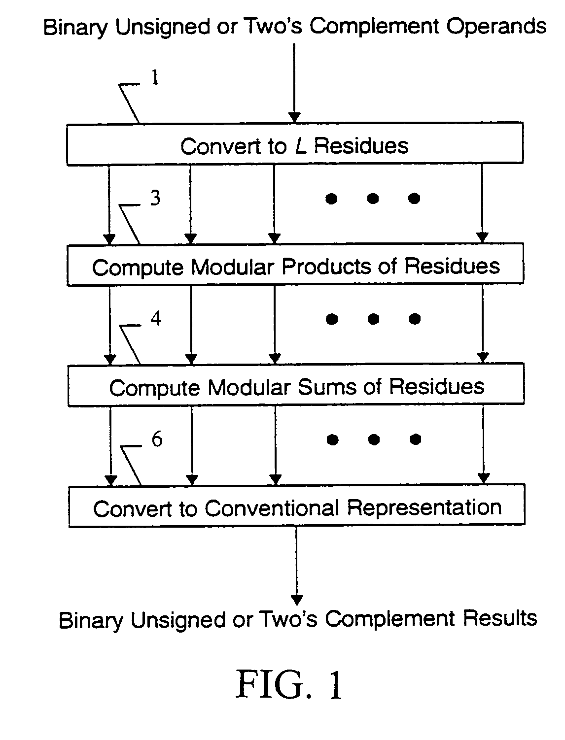
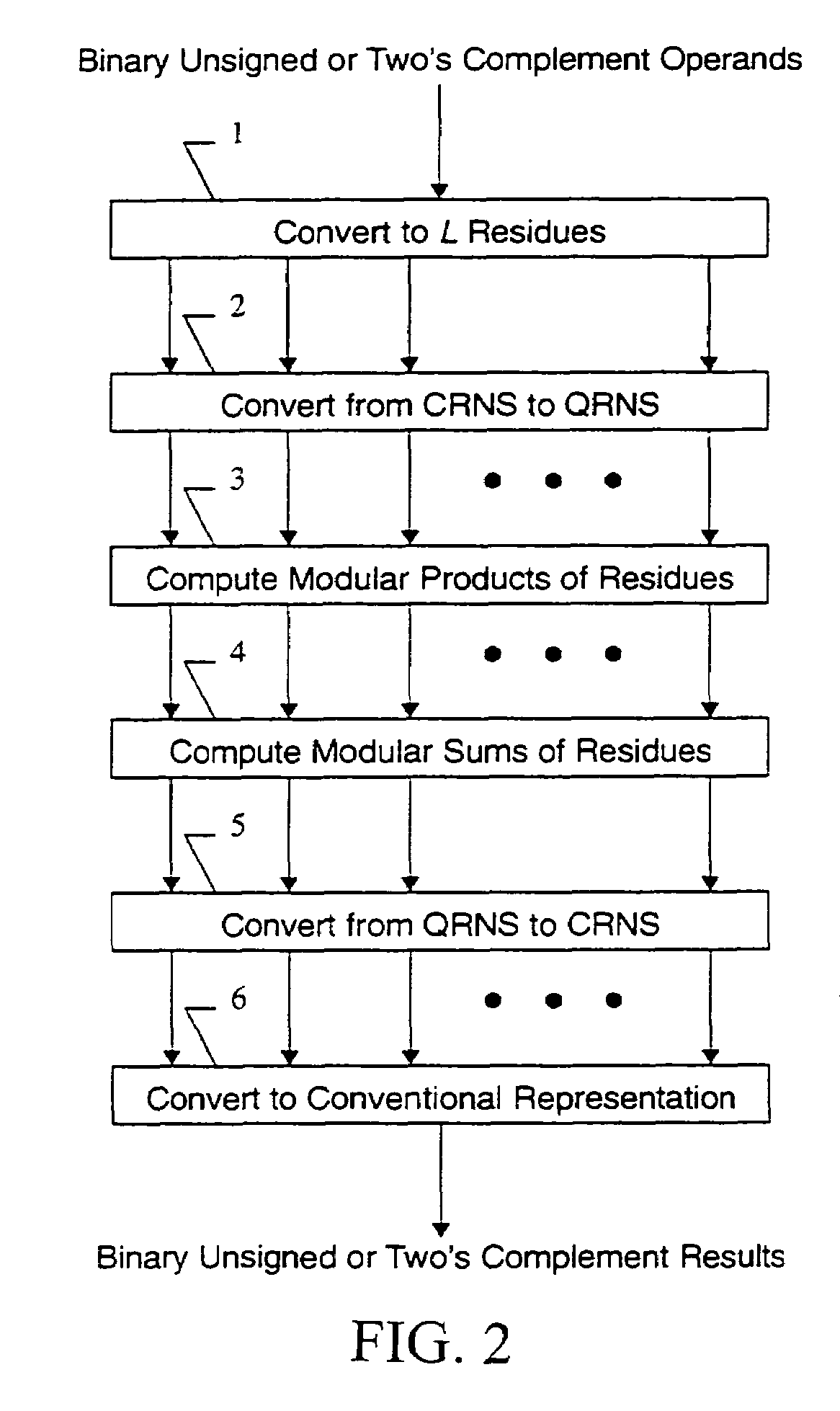
[0006]The subject invention pertains to a method and apparatus for performing computations using the Residue Number System (RNS). In a specific embodiment, a plurality of logic gates can be utilized to implement computations using the RNS. In light of recent semiconductor device scaling and design methodology changes, the subject invention can offer advantages over the use of ROMs for small table lookup functions in integrated RNS digital signal processor implementations. Some of these advantages include: logic gates can scale down in size or power better than the analog portions of the ROM circuitry, for example the differential sense amplifier; for integrated RNS implementations, small table lookup functions implemented with gates require less die area than the same functions implemented with ROMs; in general, logic gates are compatible with quiescent current test methodologies, while memory devices are not compatible with quiescent, or leakage, current test methodologies (also known as IDDQ testing); logic gates are generally scan testable whereas memory devices can require special test structures and are typically not directly compatible with scan test methodologies; and signal wires may be routed over logic gates, whereas most design methodologies do not allow signal wires to be routed over on-chip memories such that the presence of many small memories in a design may congest wire routing, potentially leading to higher design costs, slower circuit operation, greater power consumption, greater silicon die area consumption, and, thus, greater manufacturing cost.
[0007]The present invention can provide one or more of the following advantages: provide a means of implementing residue arithmetic computational circuitry with a reduced use of, or entirely without the use of, memories for table lookup operations so that the circuitry can be easily implemented using a variety of technologies, including, but not limited to, custom digital logic, standard cell logic, cell-based arrays of logic, gate arrays, field programmable gate arrays, and programmable logic devices; provide a means of implementing residue arithmetic computational circuitry that does not consume significant power in the absence of switching activity in the circuit; to provide a means of implementing residue arithmetic computational circuitry that scales directly into deep sub-micron semiconductor fabrication technologies; to provide a means of implementing residue arithmetic computational circuitry that is compatible with standard logic test methodologies (e.g., scan, IDDQ); provide a means of optimizing the mathematical functions in the residue arithmetic computational circuitry for one or more of speed, power, and area; provide a means of implementing the mathematical functions in residue arithmetic computational circuitry that allows pipelining and is fully compatible with Electronic Design Automation (EDA) methodologies for automatic pipelining; provide a means of implementing the mathematical functions in residue arithmetic computational circuitry that takes advantage of the structure of the values resulting from a mathematical function to produce an implementation that is smaller and faster than is possible with any memory-based implementation; and provide a means of implementing mathematical functions in the residue arithmetic computational circuitry that does not unduly interfere with the routing of wires on the semiconductor device.

Problems solved by technology

In the past, it has often been impractical to implement large-scale digital signal processors using a single semiconductor device due to the limitations of the amount of logic that can be placed on such a device.
In contrast, the manual design of a collection of logic gates to realize a table lookup function can be a daunting task, and the speed, area, and power characteristics are generally not fully known until the time that the circuit is designed.
Prior techniques for performing computations using RNS suffer from one or more disadvantages related to the use of memories, usually ROMs, to implement table lookup functions.
Some of these disadvantages include: memories with the required properties for use in RNS computations are not available in sufficient quantity in all ASIC implementation technologies; memories often contain analog circuitry that uses significant power even if there is no switching activity in the circuit; the analog circuitry found in most memory devices does not scale well into deep sub-micron semiconductor fabrication technologies; memories, since they are dependent upon analog circuits (e.g., differential amplifiers), can be more difficult to test than digital logic circuits, can require separate tests and test mechanisms than digital logic circuits, and are not generally compatible with leakage current (IDDQ) test methodologies; there is little or no flexibility to optimize a memory with respect to one or more of speed, power, and area; memories can be difficult to pipeline, and in many implementation technologies there is no realistic option to pipeline memory; the size of the memory is typically fixed by the number of inputs and outputs, and is essentially independent of the contents of the memory; for reliability reasons, wires unrelated to a memory are not usually allowed to pass over a memory on a semiconductor device, such that the presence of many small memories on a semiconductor device, such as would be used in an apparatus to perform computations using the RNS, can impair the ability to connect various functions, both memory and non-memory, on the device.

Method used


Image

  • Method and apparatus for performing computations using residue arithmetic
  • Method and apparatus for performing computations using residue arithmetic
  • Method and apparatus for performing computations using residue arithmetic

Examples


Embodiment Construction

Enabling Mathematical Theory

[0026]The following subsections present the mathematics which are relevant to the operation of the invention. While the mathematics are well-known, the theory is presented here so as to provide a consistent framework of notation and symbols.

The Chinese Remainder Theorem

[0027]Let S={p0, p1, p2, . . . , PL−1}, where gcd(pi,pj)=1 for all i,jε{0, 1, 2, . . . , L−1} and i≠j, wherein gcd stands for greatest common denominator. Let M=πi=0L−1pi, and let XεZ / MZ, where Z denotes the ring of integers. By the Chinese Remainder Theorem, there exists an isomorphism

φ:Z / MZZ / p0Z×Z / p1Z×Z / p2Z× . . . ×Z / pL−1Z.

The mapping φ is given by

φ(X)→(x0, x1, x2, . . . , xL−1)

where (x0, x1, x2, . . . , xL−1)εZ / p0Z×Z / p1Z×Z / p2Z× . . . ×Z / pL−1Z, and xi≡X(mod pi) for all iε{0, 1, 2, . . . L−1}. The inverse mapping is given by

φ−1[x0, x1, x2, . . . , xL−1)]→X

where

[0028]X≡⁢(∑i=0L-1⁢⁢mi⁢〈mi-I⁢xi〉Pi)⁢(mod⁢⁢M),

mi=M / pi, mimi−1≡1(mod pi), and xp denotes the value in the set {0, 1, 2, . . . , p−1} ...


PUM


Abstract

The subject invention pertains to a method and apparatus for performing computations using residue arithmetic. The subject method and apparatus can utilize logic gates for performing calculations such as multiplication by a constant, computing a number theoretic logarithm of a residue for a given base αi and modulus pi, and computing the product of two residues, modulo pi. The use of logic gates can offer advantages when compared with the use of ROMs for table look-up functions in integrated Residue Number System digital signal processor implementations.

Description

[0001]The subject invention was made with government support under a research project supported by the National Institutes Standards and Technology Cooperative Agreement No. F0NANB7H3021. The government may have certain rights in this invention.BACKGROUND OF THE INVENTION[0002]The subject invention relates to a method and apparatus for performing computations using residue arithmetic. The subject method and apparatus can utilize the Residue Number System (RNS) to implement automatic computing machinery. The use of the RNS has been proposed in Garner, H. L., “The Residue Number System,”IRE Transactions on Electronic Computers, vol. EL-8, No. 6, June 1959, pp. 140-147, and Taylor, F. J., “Residue Arithmetic: A Tutorial with Examples,”IEEE Computer, vol. 17, No. 5, May 1984, pp. 50-61. The RNS is generally used to implement automatic computing machinery for digital signal processing. Digital signal processing (DSP) is dominated by the repetitive computation of sums of products. The RNS...

Claims


Application Information

Patent Timeline
Patent Type & Authority Patents(United States)
IPC IPC(8): G06F7/38G06F7/00G06F7/72G09C1/00H03M7/18
CPCH03M7/18G06F7/729
Inventor MELLOTT, JONATHAN D.
Owner THE ATHENA GROUP
Learn More