CMOS image sensor and method for manufacturing the same

a technology of image sensor and manufacturing method, which is applied in the direction of television system, radio frequency controlled device, transistor, etc., can solve the problems of high power consumption, complicated manufacturing process of ccd, and complicated drive mode, so as to improve the characteristic of image sensor and increase the junction capacitance of a floating diffusion area

Inactive Publication Date: 2009-03-31
DONGBU ELECTRONICS CO LTD
View PDF2 Cites 0 Cited by
  • Summary
  • Abstract
  • Description
  • Claims
  • Application Information

AI Technical Summary

Benefits of technology

[0035]It is, therefore, an object of the present invention to provide a CMOS image sensor and a method for manufacturing the same, capable of improving a characteristic of the image sensor by increasing junction capacitance of a floating diffusion area.

Problems solved by technology

However, CCDs may have various disadvantages, such as a complicated drive mode, high power consumption, and so forth.
Also, the CDD is generally manufactured using multi-step photo processes, so the manufacturing process for the CCD can be complicated.
In addition, since it can be difficult to integrate certain circuits, such as a controller, a signal processor, and an analog / digital converter (A / D converter) onto a single chip of the CCD, the CCD may not be advantageous for compact-size products.
However, although the FD has no problem when a small number of electrons are carried from the photodiode, the FD cannot receive all carried electrons when a great amount of electrons are carried to the FD area (that is, when a large quantity of electrons are generated due to a great amount of light incident onto the photodiode) because the capacitor in the FD area has a relatively small capacitance.
Accordingly, since it is difficult to receive a large amount of electrons from the photodiode, the exact potential cannot be applied to the drive transistor, so that a data failure or error may occur.

Method used


Image

  • CMOS image sensor and method for manufacturing the same
  • CMOS image sensor and method for manufacturing the same
  • CMOS image sensor and method for manufacturing the same

Examples


Embodiment Construction

[0044]Hereinafter, a preferred embodiment according to the present invention will be described in detail, with reference to the following drawings.

[0045]FIG. 4 is a layout view showing a unit pixel of a 4T CMOS image sensor according to the present invention, and FIG. 5 is a sectional view taken along line IV-IV′ of FIG. 4 showing a CMOS image sensor according to the present invention.

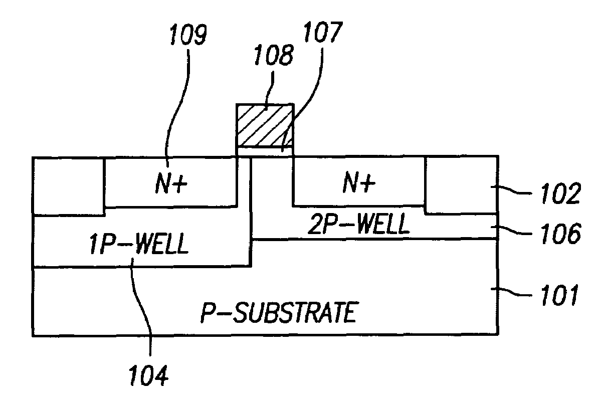
[0046]As shown in FIGS. 4 and 5, the CMOS image sensor includes an isolation layer 102 formed in an isolation area of a P type semiconductor device 101 (having defined thereon and / or therein an active area, including a photodiode (PD) area and a transistor area, and the isolation area), a first P-well area 104 in a predetermined portion of a surface of the active area of the semiconductor device 101, four gate electrodes 108, 115, 125, and 135 formed in the active area of the semiconductor device 101 with a gate insulating layer 107 between the active area and each gate electrode, N+ type diffusion are...


PUM


Abstract

Disclosed are a CMOS image sensor and a method for manufacturing the same, capable of improving the characteristics of the image sensor by increasing junction capacitance of a floating diffusion area. The CMOS image sensor generally includes a photodiode and a plurality of transistors (e.g., transfer, reset, drive, and select transistors), a first conductive type semiconductor substrate, having an active area including a photodiode area, a floating diffusion area, and a voltage input / output area, a gate electrode of each transistor on the active area, a first conductive type first well area in the semiconductor substrate corresponding to the voltage input / output area, a first conductive type second well area in the semiconductor substrate corresponding to the floating diffusion area, and a second conductive type diffusion area in the semiconductor substrate at opposed sides of each gate electrode.

Description

[0001]This application claims the benefit of Korean Application No. 10-2005-0096363, filed on Oct. 13, 2005, which is incorporated by reference herein in its entirety.BACKGROUND OF THE INVENTION[0002]1. Field of the Invention[0003]The present invention relates to a CMOS image sensor. More specifically, the present invention relates to a CMOS image sensor and a method for manufacturing the same, capable of improving characteristics of the image sensor by reducing a leakage current of a floating diffusion area.[0004]2. Description of the Related Art[0005]In general, an image sensor is a semiconductor device for converting optical images into electric signals, and it may be classified as a charge coupled device (CCD) or a CMOS image sensor.[0006]The CCD has a plurality of photodiodes (PDs), which are arranged in the form of a matrix in order to convert optical signals into electric signals. The CCD includes a plurality of vertical charge coupled devices (VCCDs) provided between photodi...

Claims


Application Information

Patent Timeline
Patent Type & Authority Patents(United States)
IPC IPC(8): H01L21/00H01L27/146H04N5/335H04N5/374
CPCH01L27/14609H01L27/14643H01L27/146
Inventor JEON, IN GYUN
Owner DONGBU ELECTRONICS CO LTD
Why Eureka
Try Eureka