Sensor system
- Summary
- Abstract
- Description
- Claims
- Application Information
AI Technical Summary
Benefits of technology
Problems solved by technology
Method used
Image
Examples
Embodiment Construction
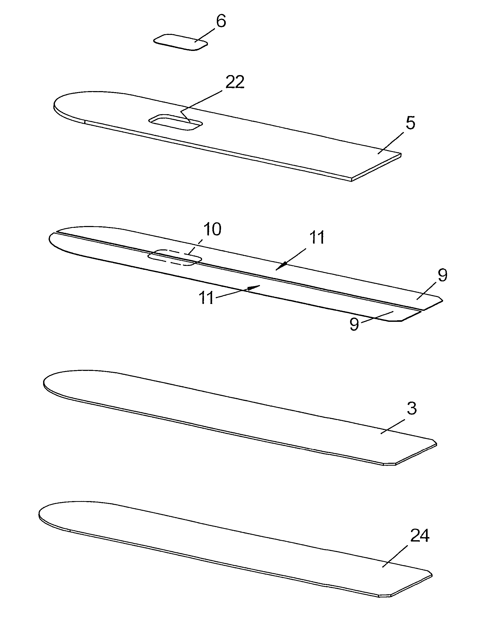
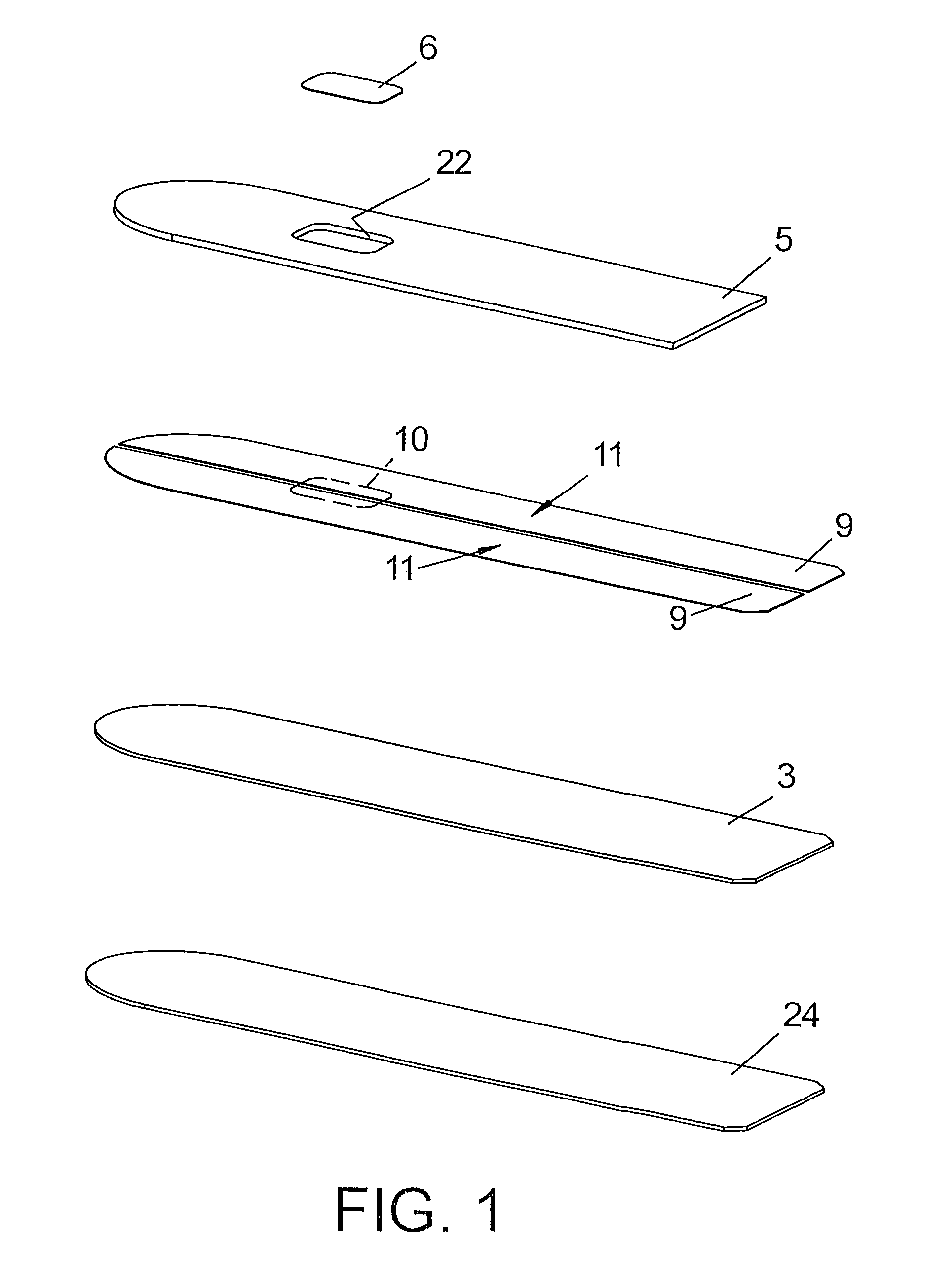
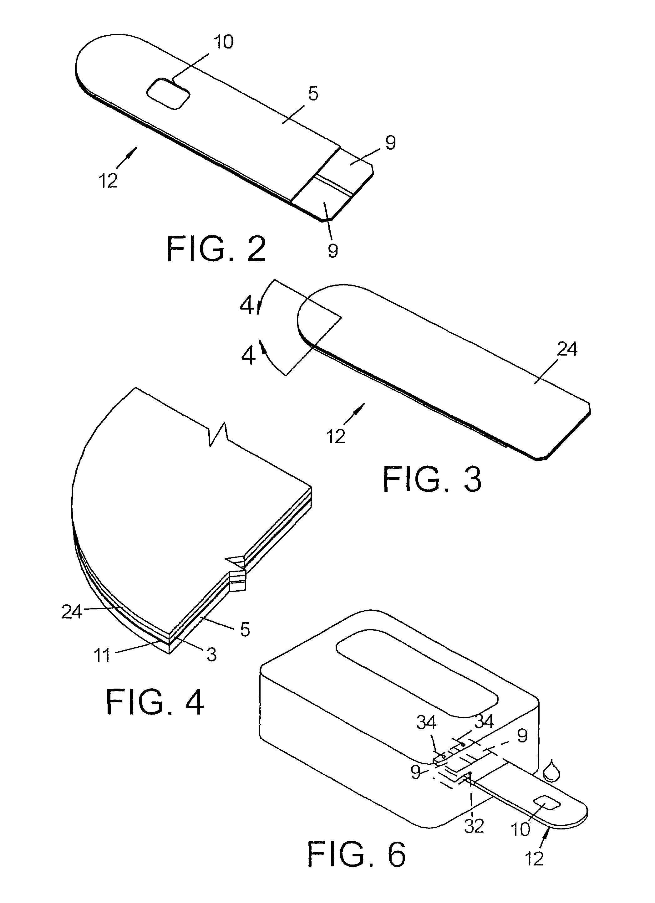
[0021]FIG. 2 is a top view of an embodiment of a sensor strip 12, FIG. 3 is a bottom view, and FIG. 1 is an exploded view. Illustrated in FIG. 1, are an electrode substrate 3, the contact pads 9 and 9, and sensing region 10, all of which are part of the electrodes 11 and 11. The electrodes are, in part, covered with a dielectric 5 exposing the sensing region 10, through hole 22 in the dielectric, and the contact pads 9 and 9. Reagent 6 is on the sensing region 10. Also illustrated is heat conducting layer 24 under the electrode substrate 3, which is most clearly illustrated in FIG. 3. In this embodiment, the sample is loaded from the top of the sensor strip via hole 22.
[0022]FIG. 4 provides a detailed illustration of a side view, from the bottom, of a portion the sensor strip 12. In this embodiment, the heat conducting layer 24 is in contact with the electrode substrate 3, which in turn is in contact with the electrodes 11. The electrodes are covered (in part) with dielectric 5.
[002...
PUM
| Property | Measurement | Unit |
|---|---|---|
| Power | aaaaa | aaaaa |
| Power | aaaaa | aaaaa |
| Power | aaaaa | aaaaa |
Abstract
Description
Claims
Application Information
 - R&D
- Intellectual Property
- Life Sciences
- Materials
- Tech Scout
- Unparalleled Data Quality
- Higher Quality Content
- 60% Fewer Hallucinations
Browse by: Latest US Patents, China's latest patents, Technical Efficacy Thesaurus, Application Domain, Technology Topic, Popular Technical Reports.
© 2025 PatSnap. All rights reserved.Legal|Privacy policy|Modern Slavery Act Transparency Statement|Sitemap|About US| Contact US: help@patsnap.com


