Liquid crystal display device with voltage compensator
a liquid crystal display and voltage compensator technology, applied in the field of liquid crystal display, can solve the problems of picture quality deterioration, picture quality deterioration of the picture displayed on the picture display part, etc., and achieve the effect of preventing a brightness differen
- Summary
- Abstract
- Description
- Claims
- Application Information
AI Technical Summary
Benefits of technology
Problems solved by technology
Method used
Image
Examples
first embodiment
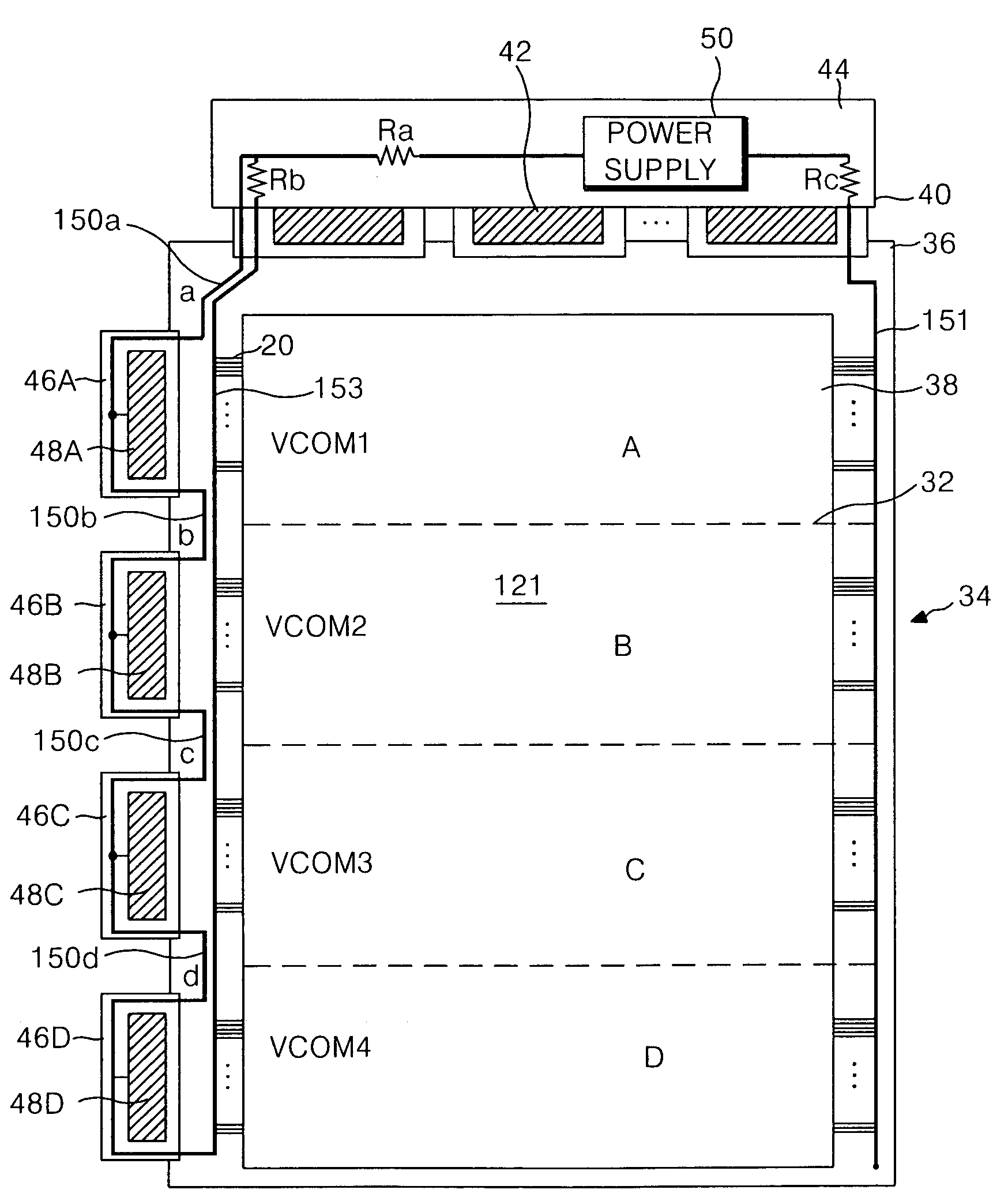
[0040]FIG. 3 illustrates a liquid crystal display device according to the present invention.
[0041]The liquid crystal display device according to the first embodiment of the present invention includes a liquid crystal display panel 34, a plurality of data TCP's 40 connected between the liquid crystal display panel 34 and a data PCB 44, a plurality of gate TCP's 46A to 46D connected to an adjacent side of the liquid crystal display panel 34, data drive IC's 42 mounted on the data TCP's 40, gate drive IC's 48A to 48D mounted in the gate TCP's 46A to 46D, a power supply 50 for generating driving voltages supplied to the gate drive IC's 48 and the data drive IC's 42, and a timing controller (not shown) controlling the gate drive IC's 48 and the data drive IC's 42.
[0042]The liquid crystal display panel 34 includes a lower substrate 36 provided with various signal lines and a thin film transistor array, an upper substrate 38 provided with a color filter array, and a liquid crystal injected...
second embodiment
[0058]FIG. 5 shows a liquid crystal display device according to the present invention.
[0059]Because the liquid crystal display device shown in FIG. 5 has the same elements as the liquid crystal display device shown in FIG. 3 except that a gate drive circuit group including a plurality of gate TCP's mounted with gate drive IC's is provided at both the left and right sides of a liquid crystal display panel (hereinafter referred to as “double gate liquid crystal display device), a detailed explanation as to the elements identical to the first embodiment will be omitted.
[0060]In the double gate liquid crystal display device shown in FIG. 5, gate lines of the liquid crystal display panel are divided into the left and right sides, and a data driving circuit converts the digital data into analog gamma voltages and applies them to all the data lines and pixels in synchronization with a scanning pulse.
[0061]A first gate drive circuit group 172 at the left side sequentially applies a scanning...
third embodiment
[0069]FIG. 6 shows a liquid crystal display device according to the present invention.
[0070]Because the liquid crystal display device shown in FIG. 6 has the same elements as the liquid crystal display device shown in FIG. 3 except that a gate drive circuit group including a plurality of gate TCP's mounted with gate drive IC's is provided at both the left and right sides of a liquid crystal display panel and the data PCB is positioned at both the upper and lower portion of a liquid crystal pattern (hereinafter referred to as “double-gate and double-source liquid crystal display device), a detailed explanation as to the elements identical to the first embodiment will be omitted.
[0071]In the double-gate and double-source liquid crystal display device shown in FIG. 6, gate lines of the liquid crystal display panel are divided into the left and right sides while data lines of the liquid crystal display panel are separated into the upper and lower portions thereof.
[0072]A first source dr...
PUM
 Abstract
Description
Claims
Application Information
 - R&D
- Intellectual Property
- Life Sciences
- Materials
- Tech Scout
- Unparalleled Data Quality
- Higher Quality Content
- 60% Fewer Hallucinations
Browse by: Latest US Patents, China's latest patents, Technical Efficacy Thesaurus, Application Domain, Technology Topic, Popular Technical Reports.
© 2025 PatSnap. All rights reserved.Legal|Privacy policy|Modern Slavery Act Transparency Statement|Sitemap|About US| Contact US: help@patsnap.com


