
Modified dual band direct conversion architecture that allows extensive digital calibration

a direct conversion and dual band technology, applied in the field of transceivers, can solve the problems of low-cost and highly integrated wireless systems, difficult or impossible to implement such filters as integrated systems, and the advantages of 802.11a come at a cost. , to achieve the effect of minimizing the transceiver area

Active Publication Date: 2008-12-09
AVAGO TECH INT SALES PTE LTD
View PDF14 Cites 25 Cited by
  • Summary
  • Abstract
  • Description
  • Claims
  • Application Information

AI Technical Summary

Benefits of technology

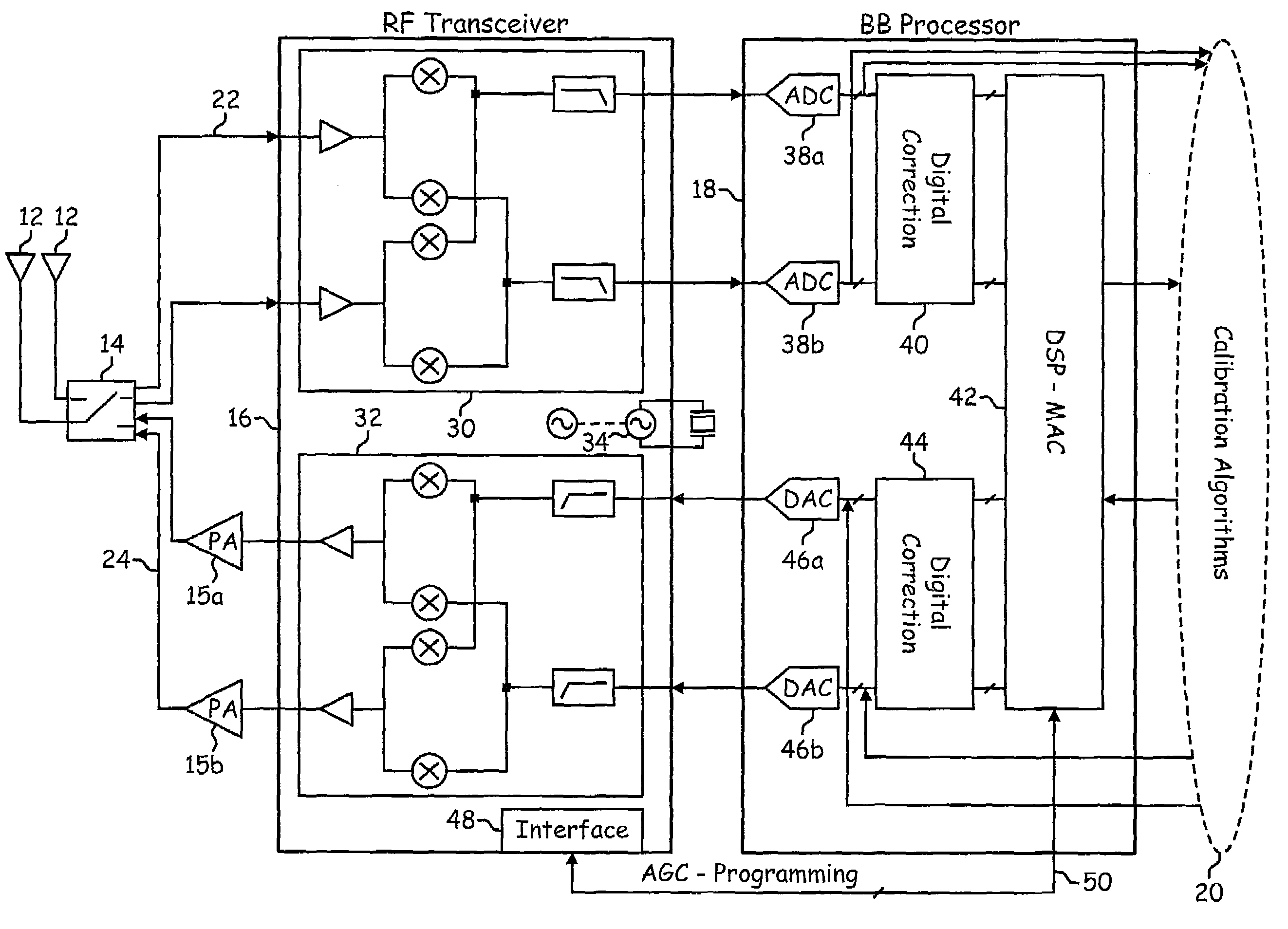
The patent describes a way to make a communication device that can work with two different signals. This design helps to make the device smaller and more efficient. It also allows for advanced calibration techniques to make sure the device works well with high-bit rate signals.

Problems solved by technology

The advantages of 802.11a come at a cost, however, as OFDM-based systems pose significant implementation challenges requiring low in-band phase noise, high linearity, accurate quadrature matching, closely matched frequency response between the I and Q signal paths, and a large dynamic range.
In addition to tight performance constraints, pricing pressures require that wireless systems be low-cost and highly integrated implementations.
It is difficult or impossible to implement such a filter as an integrated system, so external components are unavoidable.
However, such highly-integrated direct-conversion single-chip architectures suffer from well-known shortcomings that may limit their applicability.
These are problems that are also shared by other integrated architectures such as low-IF or wideband-IF, but which can be further aggravated by using CMOS technology.
For example, on the receiver side, the most common problem is the presence of DC offsets, both static and time-varying.
Static DC offset is the result of component mismatches in the signal path and local oscillator (LO) leakage at the inputs of the mixer and the low-noise amplifier (LNA) due to finite on-chip isolation.
Time-varying DC offsets, in direct conversion receivers, can be the result of self-mixing due to leakage of single-tone (CW) or frequency modulated (FM) interference to the LO port.
Similarly, second order distortion applied to CW or FM interference results in DC offset, which varies with the frequency and the power level of the received signal.
Direct down / up-conversion from / to 5 or 2.4 GHz requires quadrature LO generation at the RF carrier frequency which may result in large I / Q mismatches (including gain and phase mismatches).
Other significant problems include sensitivity to flicker noise and pulling of the voltage-controlled oscillator (VCO) by the external or on-chip power amplifier (PA).
However, such approaches may require several design iterations and can be highly sensitive to process variations, thus degrading yield and increasing overall cost, which may cancel the advantages of using CMOS integrated architectures.

Method used


Image

  • Modified dual band direct conversion architecture that allows extensive digital calibration
  • Modified dual band direct conversion architecture that allows extensive digital calibration
  • Modified dual band direct conversion architecture that allows extensive digital calibration

Examples


Embodiment Construction

[0019]The present invention relates to transceivers, and more particularly to integrated direct conversion transceivers that allow for the use of digital calibration in order to achieve performance adequate to support high bit rate modulation schemes. The following description is presented to enable one of ordinary skill in the art to make and use the invention and is provided in the context of a patent application and its requirements. Various modifications to the preferred embodiment and the generic principles and features described herein will be readily apparent to those skilled in the art. Thus, the present invention is not intended to be limited to the embodiments shown but is to be accorded the widest scope consistent with the principles and features described herein.

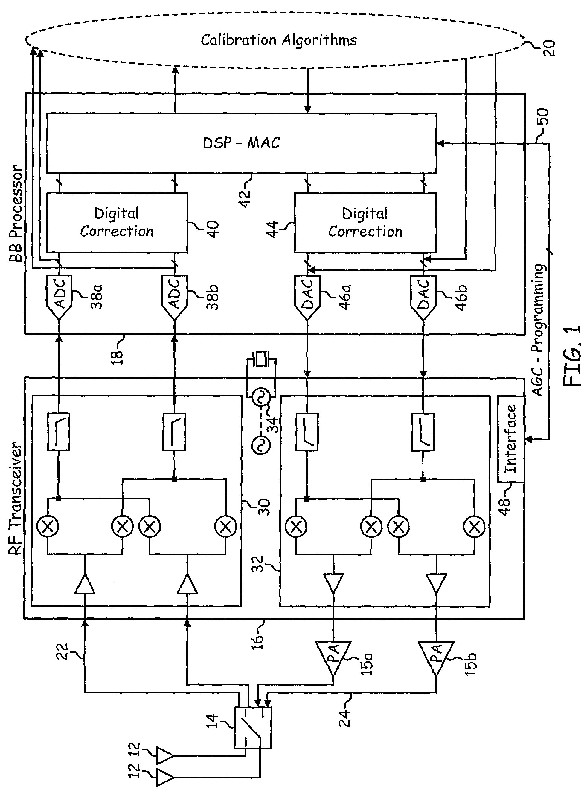
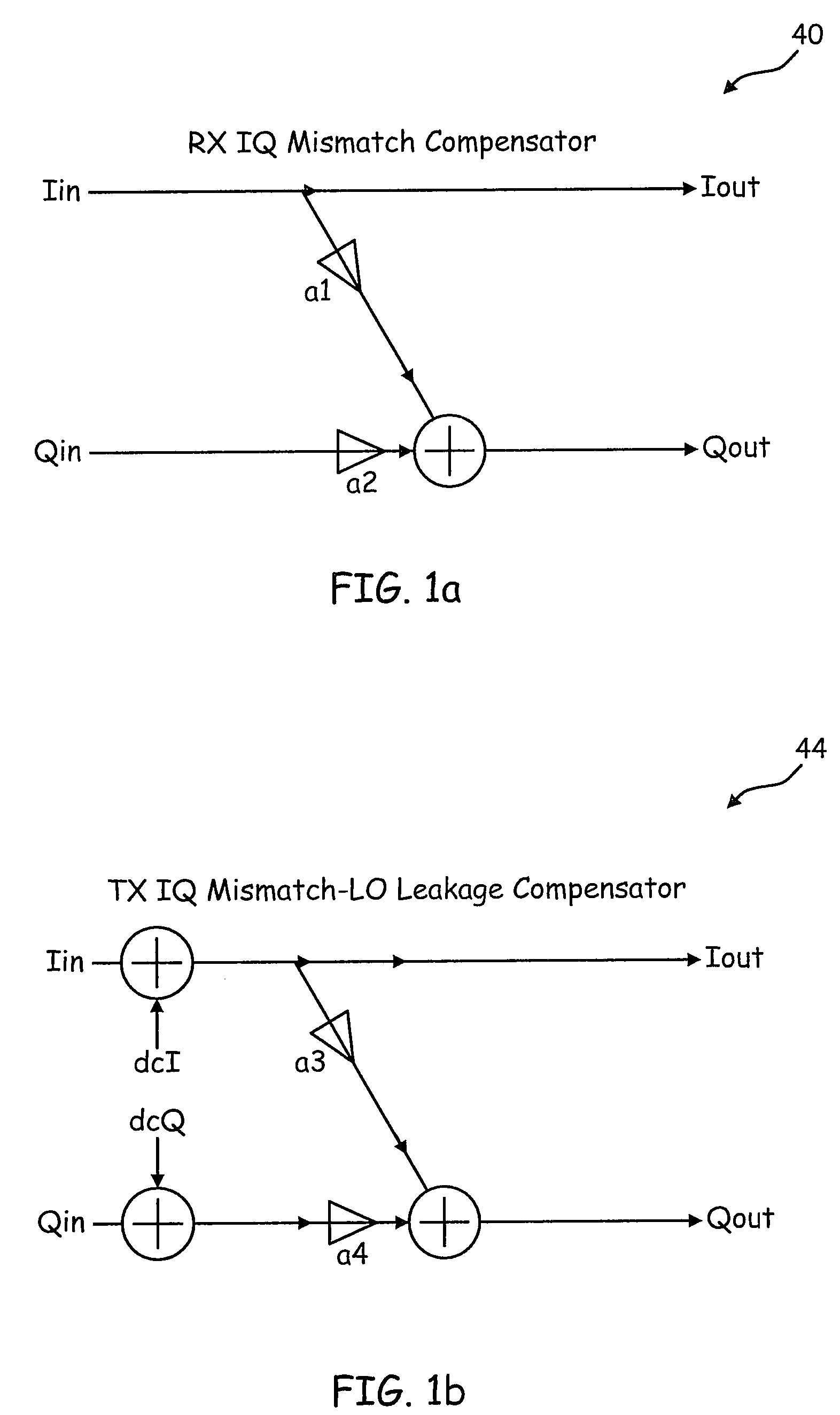
[0020]The present invention describes a direct conversion radio transceiver suitable for IEEE 802.11a / b / g applications. It is based on a system architecture that utilizes on-chip feedback paths that enable the co...


PUM


Abstract

A dual band direct conversion architecture for both the receive (RX) and transmit (TX) path of a communications transceiver that minimizes the transceiver area by sharing common circuits used in both RX and TX paths is disclosed. The transceiver also allows the use of extensive digital calibration in order to achieve performance adequate to support high bit rate modulation schemes.

Description

[0001]This application makes reference to, claims priority to, and claims the benefit of U.S. Provisional Application Ser. No. 60 / 560,950 filed on Apr. 9, 2004.FIELD OF THE INVENTION[0002]The present invention relates to transceivers, and more particularly to integrated direct-conversion transceivers that enable the use of digital calibration in order to correct for non-idealities in the system and achieve performance adequate to support high bit rate modulation schemes.BACKGROUND OF THE INVENTION[0003]One increasingly popular application for wireless systems are wireless local area networks (WLANs) of computer systems. Prominent in the field of home and business, wireless computer networks include the wireless standards known as 802.11. The first standard to be available in commercial products was 802.11b. However, increasing demand for higher capacity in the growing wireless LAN market has led to the introduction of a new generation of WLAN standards using more spectrally efficien...

Claims


Application Information

Patent Timeline
Patent Type & Authority Patents(United States)
IPC IPC(8): H04M1/00H04B1/26
CPCH04B1/30H04B1/408H04L2027/0016
Inventor VASSILIOU, IASONHARALABIDIS, NIKOSGEORGANTAS, THEODOREYAMANAKA, AKIRAVAVELIDIS, KONSTANTINOSPLEVRIDIS, SOFOKLIS
Owner AVAGO TECH INT SALES PTE LTD
Learn More