Narrow impedance conversion device

a technology of narrow impedance and conversion device, which is applied in the direction of waveguide, waveguide type device, electrical apparatus, etc., to achieve the effect of reducing the size of microelectronic parts

Active Publication Date: 2008-11-04
RENESAS ELECTRONICS CORP +8
View PDF5 Cites 0 Cited by
  • Summary
  • Abstract
  • Description
  • Claims
  • Application Information

AI Technical Summary

Benefits of technology

[0009]The impedance of the transmitted signal is converted efficiently, and the dimensions of the impedance conversion device in the directions orthogonal to the longitudinal direction of the conductors are comparatively small, permitting the impedance converting device to be formed in a confined space and in particular to be inserted into a stacked pair line. Use of this impedance conversion device can contribute to a reduction in the size of microelectronic parts.

Problems solved by technology

The disclosed device is designed for insertion into a microstrip line, however, and is too wide in the direction orthogonal to the line for insertion into a stacked pair line.

Method used


Image

  • Narrow impedance conversion device
  • Narrow impedance conversion device
  • Narrow impedance conversion device

Examples


Embodiment Construction

[0035]An impedance conversion device embodying the invention will now be described with reference to the attached drawings, in which like elements are indicated by like reference characters.

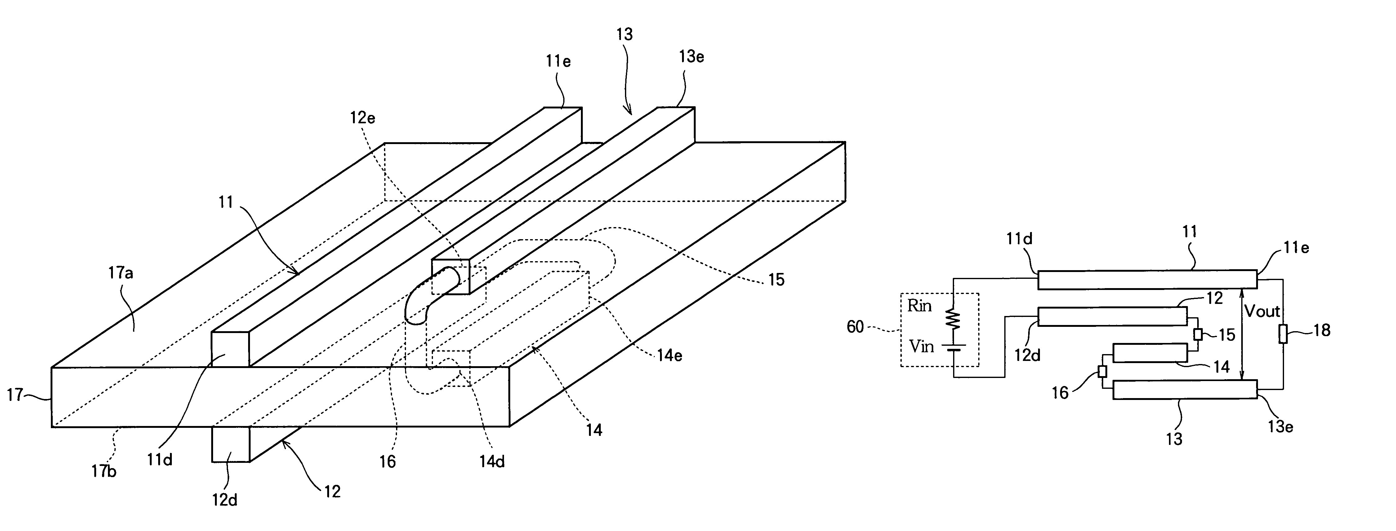
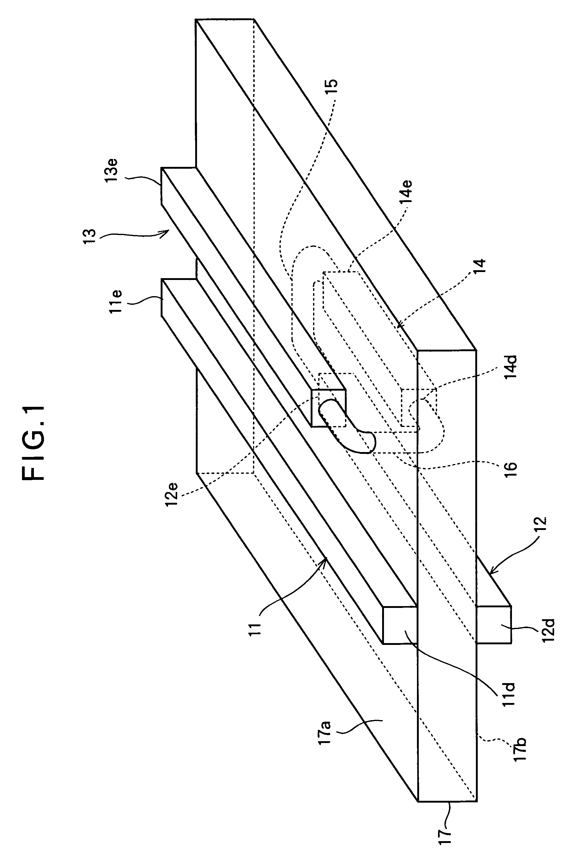
[0036]As shown in FIGS. 1-7, the impedance conversion device comprises first, second, third, and fourth strip-like conductors 11, 12, 13, 14, first and second resistors 15, 16, and a dielectric sheet 17. The first to fourth conductors 11, 12, 13, 14 extend in mutually parallel straight lines.

[0037]The dielectric sheet 17 has a first surface or upper surface 17a (uppermost in FIGS. 1 and 4-7) and a second surface or lower surface 17b. The first and third conductors 11, 13 are disposed side by side on the upper surface 17a of the dielectric sheet 17, spaced apart from each other in a direction orthogonal to their lengths and parallel to the upper surface 17a and lower surface 17b of the dielectric sheet 17. The second and fourth conductors 12, 14 are similarly disposed side by side on the lower sur...


PUM


Abstract

An impedance conversion device has four conductors arranged so that the first and second conductors form a transmission line having a first characteristic impedance, the third and fourth conductors form a transmission line having the first characteristic impedance, the first and third conductors form a transmission line having a second characteristic impedance, and the second and fourth conductors form a third transmission line having the second characteristic impedance. The second and fourth conductors are interconnected at proximate ends through a resistance equal to the first characteristic impedance. The third and fourth conductors are interconnected at proximate ends through a resistance equal to the second characteristic impedance. The lateral dimensions of the impedance conversion device are small enough to permit insertion in a stacked pair line.

Description

BACKGROUND OF THE INVENTION[0001]1. Field of the Invention[0002]The present invention relates to an impedance conversion device, and in particular to an impedance conversion device that can be inserted into a stacked pair line.[0003]2. Description of the Related Art[0004]An example of a conventional impedance conversion device that can be inserted in a transmission line is given in Japanese Patent Application Publication No. 10-224123. The disclosed device is designed for insertion into a microstrip line, however, and is too wide in the direction orthogonal to the line for insertion into a stacked pair line.SUMMARY OF THE INVENTION[0005]An object of the present invention is to provide an impedance conversion device that is narrow enough for insertion into a stacked pair line.[0006]The invented impedance conversion device comprises first, second, third, and fourth conductors, each having a first end and a second end. The conductors are arranged so that the first and second conductors...

Claims


Application Information

Patent Timeline
Patent Type & Authority Patents(United States)
IPC IPC(8): H03H7/38H01P1/16
CPCH01P5/02H01P3/08H01P1/00H01P3/00
Inventor OTSUKA, KANJIUSAMI, TAMOTSUAKIYAMA, YUTAKA
Owner RENESAS ELECTRONICS CORP
Why Eureka
Try Eureka