Soft errors handling in EEPROM devices

a technology of eeprom and soft error, which is applied in the field of semiconductor memory error handling, can solve the problems of hard error, inability to detect soft error in normal operation of the device, and shift of the programmed threshold voltage level, so as to prolong the life-expectancy of the eeprom or flash eeprom device, improve reliability, and improve performance. performance. good

Inactive Publication Date: 2008-10-14
SANDISK TECH LLC
View PDF110 Cites 7 Cited by
  • Summary
  • Abstract
  • Description
  • Claims
  • Application Information

AI Technical Summary

Benefits of technology

[0020]These and additional objects are accomplished by improvements in solid-state memory systems such as EEPROM and Flash EEPROM systems and in techniques that allow simple and effective handling of errors and defects, so that non-volatile, solid-state memory, even if imperfect, may be used reliably and economically as a mass storage.
[0027]The “scrubbing” technique as prescribed by the invention is a very powerful, yet simple way to improve the reliability and extend the life-expectancy of the EEPROM or Flash EEPROM devices. By “amortizing” the scrubbing operation of the whole array over many normal operations, the memory device suffers very little degradation in performance.

Problems solved by technology

As the memory device is used, the threshold level of a cell not subjected to erase or program operations may lose margin, thereby producing a soft error not readily detectable by normal operations of the device.
The perturbation may cause electric charge to leak either into or out of the floating gate of the perturbed cells, again resulting in a shifting of the programmed threshold voltage levels.
If enough of these perturbations accumulate on a cell, a hard error could develop.

Method used


Image

  • Soft errors handling in EEPROM devices
  • Soft errors handling in EEPROM devices
  • Soft errors handling in EEPROM devices

Examples


Embodiment Construction

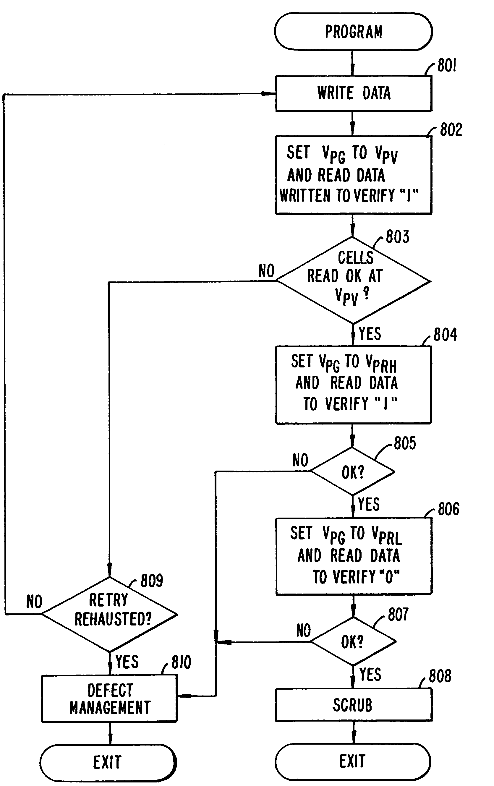
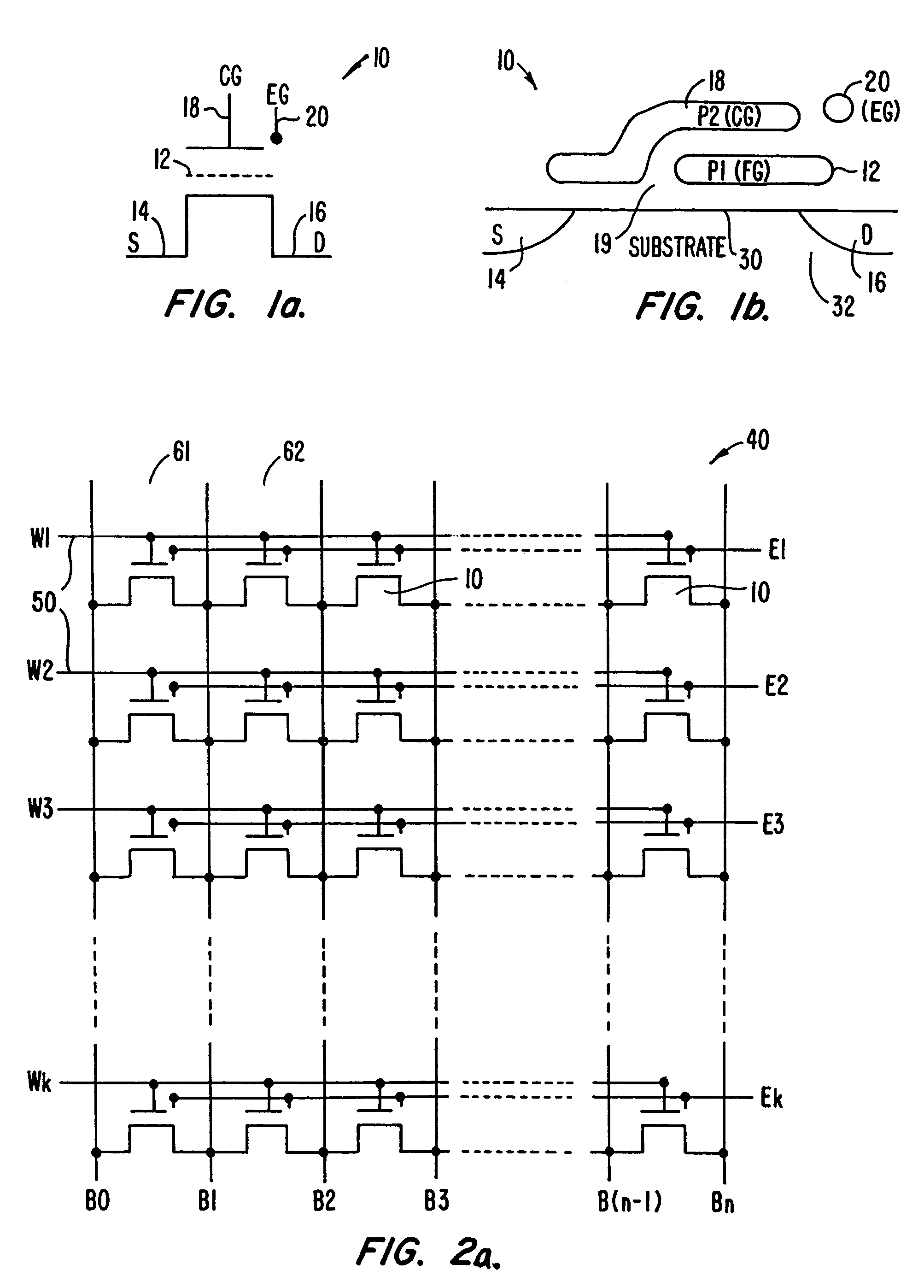
[0044]FIG. 1a illustrates schematically a typical EEPROM cell 10 having a floating gate 12, a source 14, a drain 16, a control gate 18 and an erase gate 20. An exemplary EEPROM structure is generally illustrated in the cross-sectional view of FIG. 1b. The memory cell 10 is formed on a lightly p-doped substrate 30. The source 14 and the drain 16 are formed as two heavily n-doped implanted regions. The floating gate 12, and the control gate 18 are generally made of polysilicon material and insulated from each other and from other conductive elements by regions of dielectric material 19.

[0045]The memory cell 10 is programmed by transferring electrons from the substrate 30 to the floating gate 12. In the example cell of FIG. 1b, the electric charge in the floating gate 12 is increased by electrons forced across the dielectric region 19 from the channel 32 near the drain 16 and into the floating gate 12. Electric charge is removed from the floating gate 12 during an erase operation throu...


PUM


Abstract

Soft errors occur during normal use of a solid-state memory such as EEPROM or Flash EEPROM. A soft error results from the programmed threshold voltage of a memory cell being drifted from its originally intended level. The error is initially not readily detected during normal read until the cumulative drift becomes so severe that it develops into a hard error. Data could be lost if enough of these hard errors swamps available error correction codes in the memory. A memory device and techniques therefor are capable of detecting these drifts and substantially maintaining the threshold voltage of each memory cell to its intended level throughout the use of the memory device, thereby resisting the development of soft errors into hard errors.

Description

CROSS-REFERENCE TO RELATED APPLICATION[0001]This application is a continuation of application Ser. No. 09 / 437,078, filed Nov. 9, 1999, which is a continuation of application Ser. No. 08 / 908,265, filed Aug. 7, 1997, which is a continuation of application Ser. No. 08 / 406,677, filed Mar. 20, 1995, now Pat. No. 5,657,332, which is a divisional of application Ser. No. 07 / 886,030, filed May 20, 1992, now abandoned, which applications are incorporated herein in their entirety by this reference.TECHNICAL FIELD[0002]This invention relates generally to error handling in semiconductor memories. In one specific aspect, this invention relates to improving the reliability of memory devices. In another specific aspect, this invention is related to continual detection and correction of potential data errors in memories such EEPROM or Flash EEPROM.BACKGROUND OF THE INVENTION[0003]While mass data backup storage in data processing systems has so far relied on magnetic disk drives, the relatively high ...

Claims


Application Information

Patent Timeline
Patent Type & Authority Patents(United States)
IPC IPC(8): G11C29/00G06F11/10G11C16/10G11C29/50G11C29/52
CPCG11C16/10G11C16/3431G11C29/028G11C29/50G11C29/50004G11C29/52G06F11/1068G06F11/1072G06F2201/81G11C16/04G11C2029/5004G11C2029/5006
Inventor AUCLAIR, DANIEL L.CRAIG, JEFFREYMANGAN, JOHN S.NORMAN, ROBERT D.GUTERMAN, DANIEL C.MEHROTRA, SANJAY
Owner SANDISK TECH LLC
Why Eureka
Try Eureka