
Use of expanding material oxides for nano-fabrication

a nano-scale, oxide technology, applied in the direction of fixed micro-structural devices, microelectromechanical systems, electrical apparatus, etc., can solve the problems of increasing the difficulty of insulate certain regions of devices, difficult to achieve at the nano-scale level, and general approach is difficult to implement, so as to achieve localized pressurization, reduce the cost of insulate, and improve the effect of economic benefits

Active Publication Date: 2008-06-03
SAMSUNG ELECTRONICS CO LTD
View PDF8 Cites 0 Cited by
  • Summary
  • Abstract
  • Description
  • Claims
  • Application Information

AI Technical Summary

Benefits of technology

This patent describes a method for making nano-dimensional structures by depositing a layer of material onto a substrate and creating an oxidizable layer next to it. This oxidizable layer interacts with the deformable material to apply pressure to it. The method is easy to use, economical, and allows for localized pressurization. This method is much more efficient and effective than previous methods.

Problems solved by technology

With increasing complexity of nanostructures, it will be more and more difficult to insulate certain regions of the device, while leaving others intact or exposed to the environment.
However, this general approach is difficult to implement when coverage of the device areas adjacent to the area being insulated is undesirable because it may interfere with the device's operation.
In such cases, very precise masking processes (alignment, deposition, etc.) are required, which would be difficult to achieve at the nanoscale level.
Such an edge would be very difficult, if not impossible, to insulate using the traditional mask and deposit approach, Without depositing material on the top face of the structure, which may be undesirable.
While this method can be satisfactory for research purposes, it is not suitable for large-scale fabrication.
This is due to the fact that this method is extremely slow and cannot be applied in parallel.
Also, the applied force is limited by the mechanical hardness of the tip.

Method used


Image

  • Use of expanding material oxides for nano-fabrication
  • Use of expanding material oxides for nano-fabrication
  • Use of expanding material oxides for nano-fabrication

Examples


Embodiment Construction

[0026]For clarity of the description, the drawings are not drawn to a uniform scale. In particular, vertical and horizontal scales may differ from each other and may vary from one drawing to another. In this regard, directional terminology, such as “top,”“bottom,”“front,”“back,”“leading,”“trailing,” etc., is used with reference to the orientation of the drawing figure(s) being described. Because components of the invention can be positioned in a number of different orientations, the directional terminology is used for purposes of illustration and is in no way limiting.

[0027]The term “oxidation” is used in this specification and the appended claims to mean electrochemical oxidization (anodization) or thermal oxidation of an oxidizable material (such as an oxidizable metal). “Anodization” is performed by employing the oxidizable material as an anode in an electrolytic cell and by operating the electrolytic cell with voltage and current suitable to partially or fully oxidize the materi...


PUM


Abstract

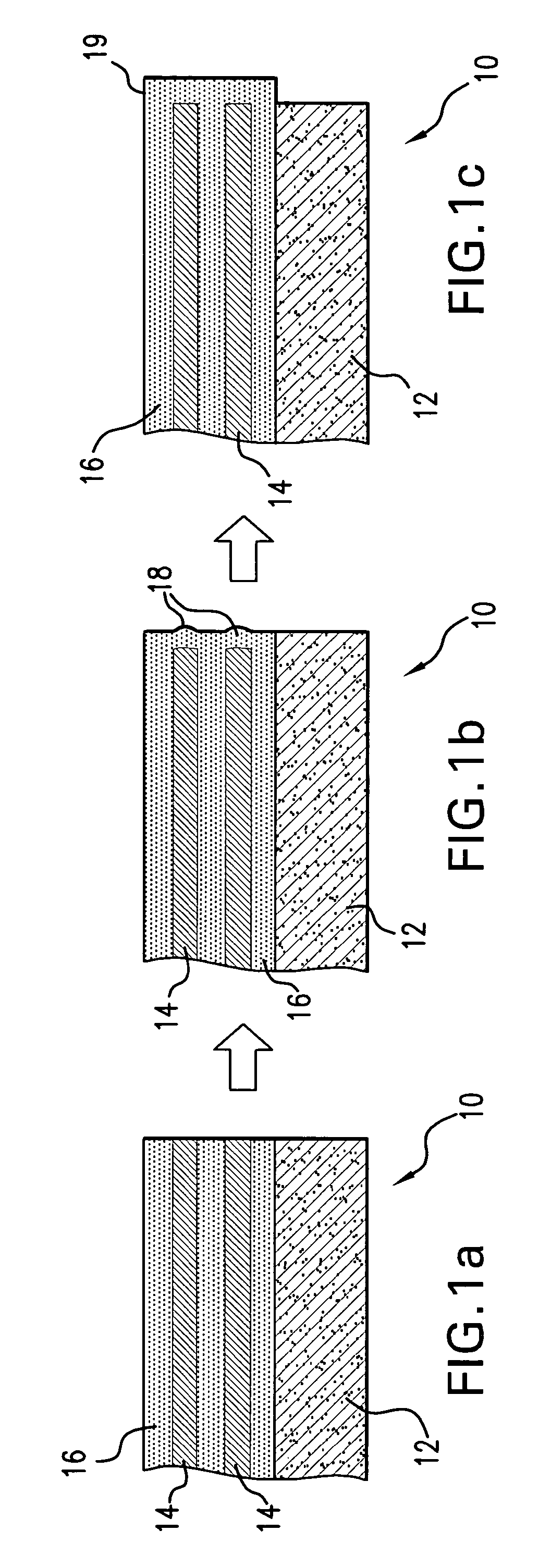
This invention relates to a method of fabricating nano-dimensional structures, comprising: depositing at least one deformable material upon a substrate such that the material includes at least one portion; and creating an oxidizable layer located substantially adjacent to the deposited deformable material such that at least a portion of the oxidized portion of the oxidizable layer interacts with the at least one portion of the deformable material to apply a localized pressure upon the at least one portion of the deformable material.

Description

BACKGROUND OF THE INVENTION[0001]1. Field of the Invention[0002]This invention relates to a method of fabricating nano-dimensional structures, comprising: depositing at least one deformable material upon a substrate such that the material includes at least one portion; and creating an oxidizable layer located substantially adjacent to the deposited deformable material such that at least a portion of the oxidized portion of the oxidizable layer interacts with the at least one portion of the deformable material to apply a localized pressure upon the at least one portion of the deformable material.[0003]2. Description of the Related Art[0004]Prior to the present invention, as set forth in general terms above and more specifically below, it is known, that industrial interest in materials having structural and functional features with nanoscale dimensions has been growing rapidly. Nano-structures have been fabricated by semiconductor processing techniques including patterning techniques ...

Claims


Application Information

Patent Timeline
Patent Type & Authority Patents(United States)
IPC IPC(8): H01L21/20H01L21/36
CPCB81B1/00B82Y10/00B81B2203/0361Y10S977/70
Inventor MARDILOVICH, PETERKORNILOVICH, PAVELHOFFMAN, RANDY
Owner SAMSUNG ELECTRONICS CO LTD
Learn More