
Modular probe card

Inactive Publication Date: 2008-05-13
CHIPMOS TECH INC
View PDF4 Cites 19 Cited by
  • Summary
  • Abstract
  • Description
  • Claims
  • Application Information

AI Technical Summary

Benefits of technology

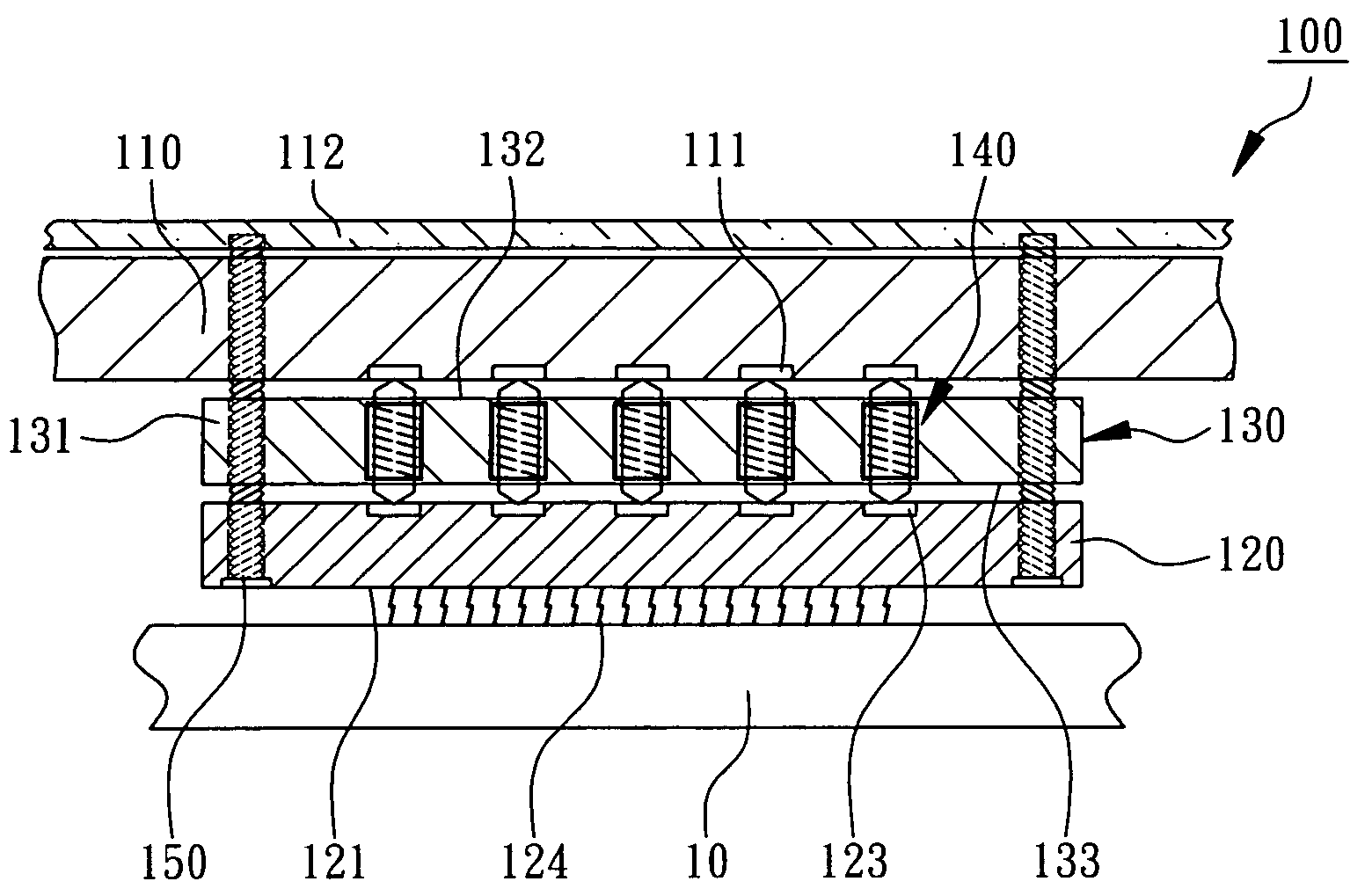
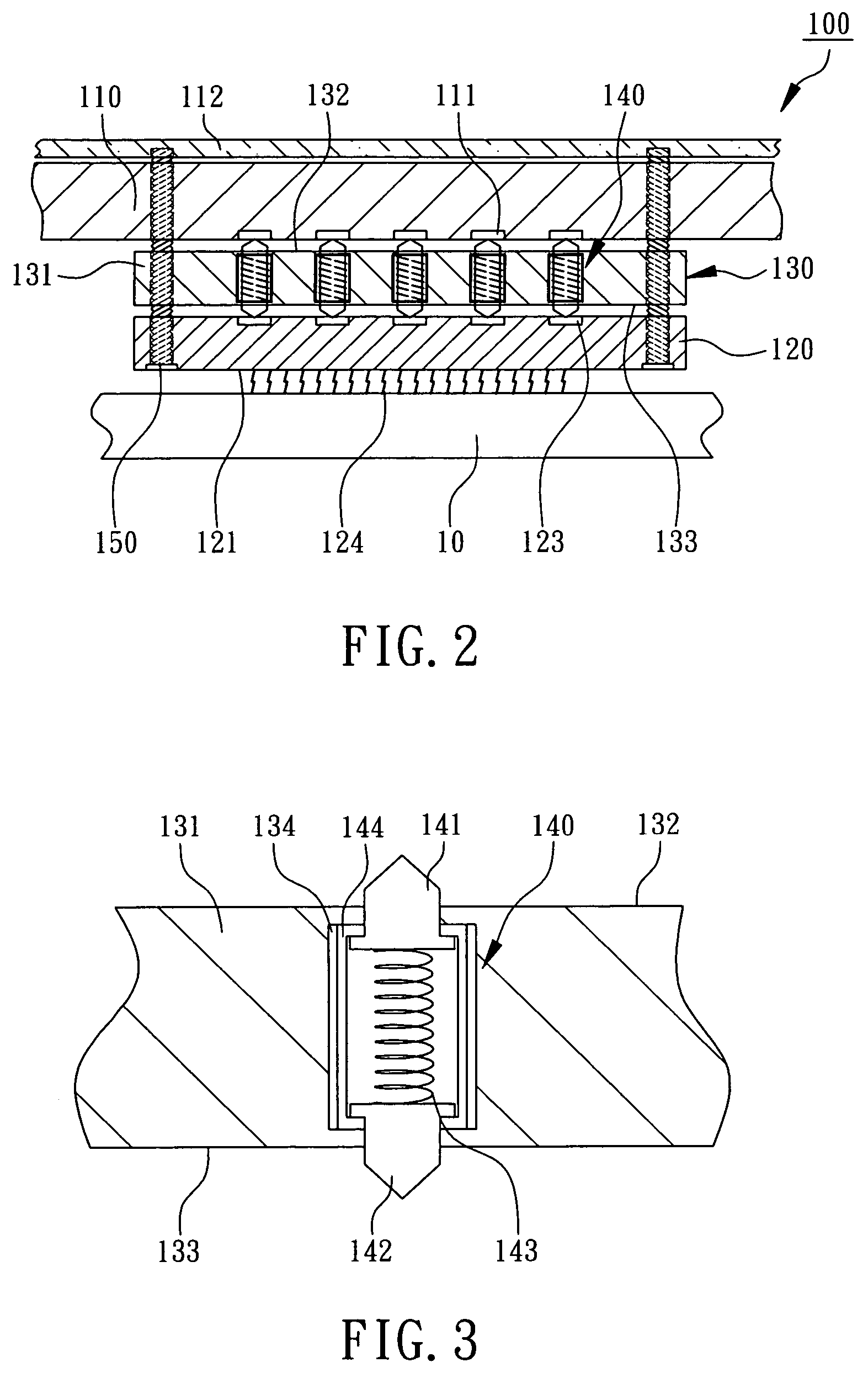
The present invention provides a modular probe card with an interposer that has pogo pins with multiple contact points that can elastically contact the contact pads of the printed circuit board, even if the contact pads are not perfectly aligned. This eliminates electrical connection failures that might occur with conventional interposers. Additionally, the pogo pins have a low elastic extruded height, allowing them to fully contact the printed circuit board pads while still being tolerant to warping of the printed circuit board and the probe head. This ensures reliable electrical connections.

Problems solved by technology

Even though the contact pads of the printed circuit board have poor coplanarity, the first contact points of the pogo pins still can elastically contact with the corresponding contact pads of the printed circuit board due to their elastic characters.

Method used


Image

  • Modular probe card
  • Modular probe card
  • Modular probe card

Examples


Embodiment Construction

[0013]Please refer to the attached drawings, the present invention will be described by means of embodiment(s) below.

[0014]According to the embodiment of the present invention, a modular probe card is illustrated as shown in FIG. 1 and FIG. 2. The modular probe card 100 comprises a printed circuit board 110, a probe head 120, and an interposer 130 where the printed circuit board 110 has a plurality of first contact pads 111, and the probe head 120 has a plurality of second contact pads 123. The printed circuit board 110 is made from FR-4, FR-5, or BT resin with a multi-layer circuit design for mounting to a test head of an IC tester. The probe head 120 has a contact surface 121 and a joint surface 122 where a plurality of probes 124 are formed on the contact surface 121 such as vertical MEMS probes or elastic probes to probe a wafer 10 under test (as shown in FIG. 2), or other integrated circuits such as tape carrier packages (TCP), or chip-on-film packages (COF). The second contact...


PUM


Abstract

A modular probe card comprises a printed circuit board, an interposer, and a probe head where the printed circuit board has a plurality of first contact pads, the probe head has a plurality of second contact pads. The interposer is disposed between the printed circuit board and the probe head where the interposer includes a substrate and a plurality of pogo pins. The substrate has a first surface, a second surface, and a plurality of through holes penetrating from the first surface to the second surface. The pogo pins are secured in the through holes of the substrate. Each of the pogo pins has a first contact point, a second contact point, and a spring therebetween, whereby the first contact points are elastically extruded from the first surface to contact the first contact pad, and the second contact points are elastically extruded from the second surface to contact the second contact pad, so as to overcome the poor electrical connections between the printed circuit board and the probe head through the interposer due to poor coplanarity of the first contact pads of the printed circuit board.

Description

FIELD OF THE INVENTION[0001]The present invention relates to tooling for testing IC, and more particularly, to a modular probe card.BACKGROUND OF THE INVENTION[0002]During the fabrication of integrated circuits, ICs, a plurality of IC chips are fabricated on a semiconductor wafer. After singulation, the individual chips are packaging into IC components. To ensure good functions and designed performance, there are several testing steps involved before sending to the customers.[0003]Testing of IC chips on a wafer before singulation is called chip probing or wafer sorting. Since the design of IC chips becomes more complicated, therefore, through chip probing or wafer sorting, the yield of the fabricated wafer can be determined then feed back to IC fab for process improvement.[0004]An IC tester for chip probing or wafer sorting has a test head on which a probe card is installed as a signal transmitting medium between the tester and the wafer under test.[0005]As revealed in U.S. Pat. No....

Claims


Application Information

Patent Timeline
Patent Type & Authority Patents(United States)
IPC IPC(8): G01R1/073
CPCG01R1/07378
Inventor LEE, YI-CHANGLIU, AN-HONGHUANG, HSIANG-MINGLEE, YAO-JUNGWANG, YEONG-HER
Owner CHIPMOS TECH INC
Learn More