Stable organic light-emitting devices using aminoanthracenes
a technology of organic light-emitting devices and aminoanthracenes, which is applied in the direction of discharge tube luminescnet screens, other domestic articles, natural mineral layered products, etc., can solve the problems of insufficient stability, persistent low operational stability, and many desirable practical applications, and achieve low drive voltage , excellent luminance efficiency, and high operational stability
- Summary
- Abstract
- Description
- Claims
- Application Information
AI Technical Summary
Benefits of technology
Problems solved by technology
Method used
Image
Examples
working device examples 1-7
[0119]The present invention and its advantages can be better appreciated by the following inventive and comparative examples. In these examples, the thickness of the organic layers and the doping concentration were controlled and measured in situ using calibrated thickness monitors (INFICON IC / 5 Deposition Controller). The electroluminescence characteristics of all the fabricated devices were evaluated using a constant current source (KEITHLEY 2400 SourceMeter) and a photometer (PHOTO RESEARCH SpectraScan PR 650) at room temperature.
example 1
Comparative Example
[0120]The preparation of a conventional OLED is as follows: A ˜1.1 mm thick glass substrate coated with a transparent ITO conductive layer was cleaned and dried using a commercial glass scrubber tool. The thickness of ITO is about 42 nm and the sheet resistance of the ITO is about 68 Ω / square. The ITO surface was subsequently treated with oxidative plasma to condition the surface as an anode. A layer of CFx, 1 nm thick, was deposited on the clean ITO surface as the HIL by decomposing CHF3 gas in an RF plasma treatment chamber. The substrate was then transferred into a vacuum deposition chamber (TROVATO MFG. INC) for deposition of all other layers on top of the substrate.
[0121]The following layers were deposited in the following sequence by evaporation from a heated boat under a vacuum of approximately 10−6 Torr: (1) a hole-transport layer, 75 nm thick, including NPB; (2) a luminescent layer, 37.5 nm thick, including Alq as the sole host material and 0.6% DPQA as t...
example 2
Inventive Example
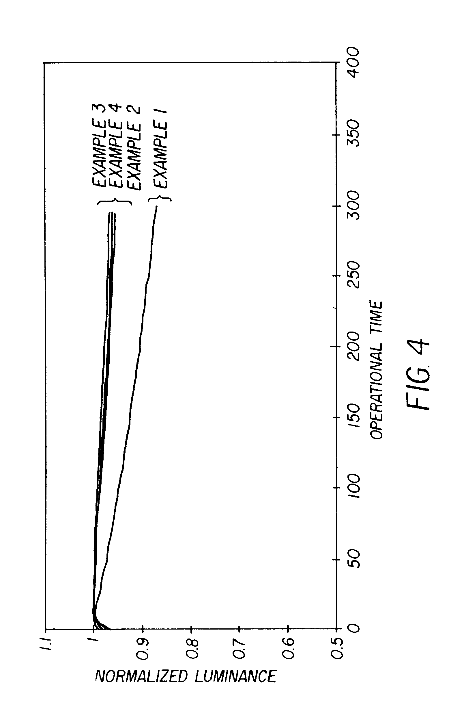
[0124]An OLED device similar to that of Comparative Example 1 was constructed, except that in the luminescent layer, Compound I is the material for the first host component, Alq is the material for the second host component, and DPQA is the fluorescent dopant. The relative amounts of Compound I, Alq, and DPQA on a volume basis are in the ratio 25.2:74.2:0.6. The EL characteristics of this device are also shown in Table II. This device requires a drive voltage of 8.3 V to pass 20 mA / cm2. Its luminance is 1857 cd / m2 and its luminance efficiency is 9.3 cd / A. When compared to Example 1, the efficiency is slightly higher and the voltage is lower. Luminance decay vs. operational time is shown in FIG. 4. After 300 hours operation, the luminance dropped by only about 5%.
PUM
| Property | Measurement | Unit |
|---|---|---|
| current density | aaaaa | aaaaa |
| dipole moment | aaaaa | aaaaa |
| dipole moment | aaaaa | aaaaa |
Abstract
Description
Claims
Application Information
 - R&D
- Intellectual Property
- Life Sciences
- Materials
- Tech Scout
- Unparalleled Data Quality
- Higher Quality Content
- 60% Fewer Hallucinations
Browse by: Latest US Patents, China's latest patents, Technical Efficacy Thesaurus, Application Domain, Technology Topic, Popular Technical Reports.
© 2025 PatSnap. All rights reserved.Legal|Privacy policy|Modern Slavery Act Transparency Statement|Sitemap|About US| Contact US: help@patsnap.com


