Multi stack packaging chip and method of manufacturing the same

a technology of packaging chip and stack structure, which is applied in the direction of semiconductor devices, electrical devices, micro-electromechanical systems, etc., can solve the problems of wire bonding deteriorating a chip performance, chip may not be manufactured in a stack structure, and the element performing specific functions such as microstructures are easily broken by foreign materials or outer impacts

Active Publication Date: 2008-02-26
SAMSUNG ELECTRONICS CO LTD
View PDF12 Cites 8 Cited by
  • Summary
  • Abstract
  • Description
  • Claims
  • Application Information

AI Technical Summary

Problems solved by technology

In general, elements performing specific functions like microstructures such as integrated chips (ICs), hybrid chips, radio frequency (RF) systems, or micro electro-mechanical systems (MEMSs) and actuators are easily broken by foreign materials or outer impacts.
However, the wire bonding deteriorates a performance of a chip due to an increase in a parasitic capacitance of the wires 30.
Thus, the chip may not be manufactured in a stack structure.

Method used


Image

  • Multi stack packaging chip and method of manufacturing the same
  • Multi stack packaging chip and method of manufacturing the same
  • Multi stack packaging chip and method of manufacturing the same

Examples


Embodiment Construction

[0029]Certain exemplary embodiments of the present invention will now be described in greater detail with reference to the accompanying drawings.

[0030]In the following description, same drawing reference numerals are used for the same elements even in different drawings. The matters defined in the description such as a detailed construction and elements are nothing but the ones provided to assist in a comprehensive understanding of the invention. Thus, it is apparent that the present invention can be carried out without those defined matters. Also, well-known functions or constructions are not described in detail since they would obscure the invention in unnecessary detail.

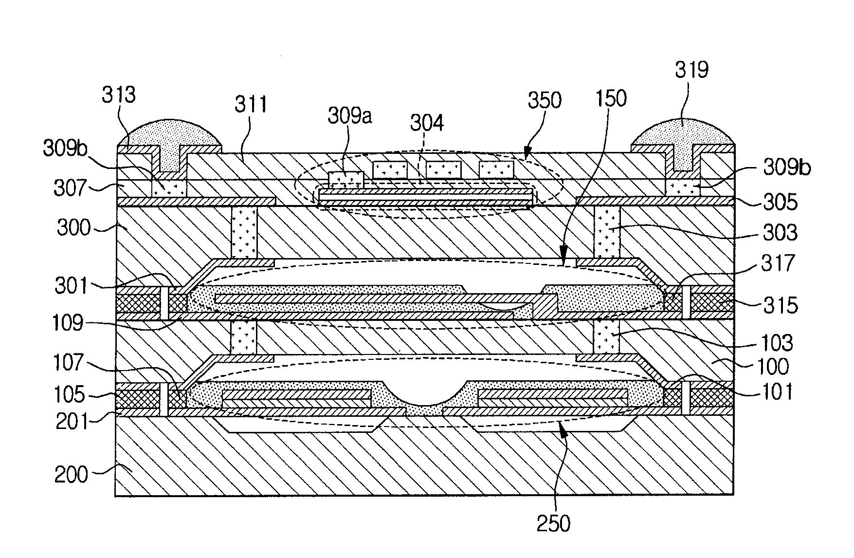
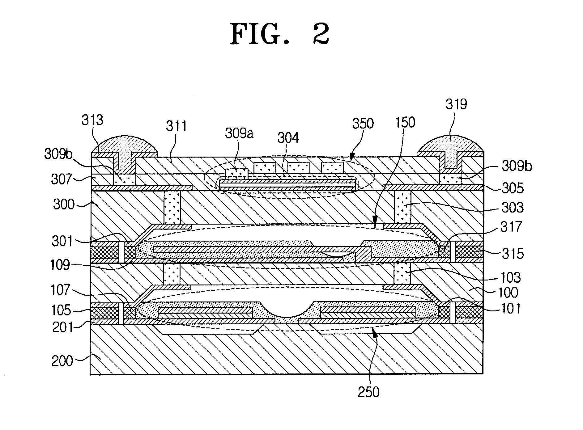
[0031]FIG. 2 is a cross-sectional view of a multi stack packaging chip according to an exemplary embodiment of the present invention. Referring to FIG. 2, the multi stack packaging chip includes a base wafer 200, at least one first circuit element 250 formed on the base wafer 200, a first cap wafer 100 packaging t...


PUM


Abstract

A multi stack packaging chip and a method of manufacturing the chip are provided. The method includes forming at least one second circuit element on a first wafer; forming a second wafer having a cavity and a one third circuit element formed opposite to the cavity; forming a solder on the second wafer; and combining the second wafer with the first wafer so that the second circuit element and the cavity correspond. The chip includes a flip-chip packaged chip in which a first circuit element is packaged using a first wafer; a second circuit element formed on the first wafer; a second wafer having a cavity and combined with the first wafer so that the cavity and the second circuit element correspond; a third circuit element formed on the second wafer; and a solder formed on the second wafer, the solder electrically coupling the second wafer to a packaging substrate.

Description

CROSS-REFERENCE TO RELATED APPLICATIONS[0001]This application claims benefit from Korean Patent Application No. 2005-38950 filed on May 10, 2005 in the Korean Intellectual Property Office, the entire disclosure of which is incorporated herein by reference.BACKGROUND OF THE INVENTION[0002]1. Field of the Invention[0003]The present invention relates to a multi stack packaging chip and a method of manufacturing the same, and more particularly, to a multi stack packaging chip generated by forming and packaging a circuit element on a cap wafer of a flip-chip packaged chip and a method of manufacturing the same.[0004]2. Description of the Related Art[0005]In general, elements performing specific functions like microstructures such as integrated chips (ICs), hybrid chips, radio frequency (RF) systems, or micro electro-mechanical systems (MEMSs) and actuators are easily broken by foreign materials or outer impacts. Thus, circuit elements must be packaged to be prevented from being broken by...

Claims


Application Information

Patent Timeline
Patent Type & Authority Patents(United States)
IPC IPC(8): H01L23/02H01L21/00
CPCB81B7/007B81C1/0023H01L23/04H01L23/49816H01L25/0657H01L25/50B81C2203/0118H01L2224/48463H01L2225/06513H01L2225/06541H01L2225/06586H01L2924/01029H01L2924/01078H01L2924/01079H01L2924/16235H01L2924/19041H01L2924/00014H01L24/48H01L2924/01322H01L2224/45099H01L2224/45015H01L2924/207H01L23/12
Inventor HWANG, JUN-SIKKIM, WOON-BAEMOON, CHANG-YOULLEE, MOON-CHULJUNG, KYU-DONG
Owner SAMSUNG ELECTRONICS CO LTD
Why Eureka
Try Eureka