Reference-less clock circuit
a clock circuit and reference-less technology, applied in the direction of optical radiation measurement, pulse technique, instruments, etc., can solve the problems of creating additional expense and application requirements for this type of frequency accuracy
- Summary
- Abstract
- Description
- Claims
- Application Information
AI Technical Summary
Benefits of technology
Problems solved by technology
Method used
Image
Examples
Embodiment Construction
)
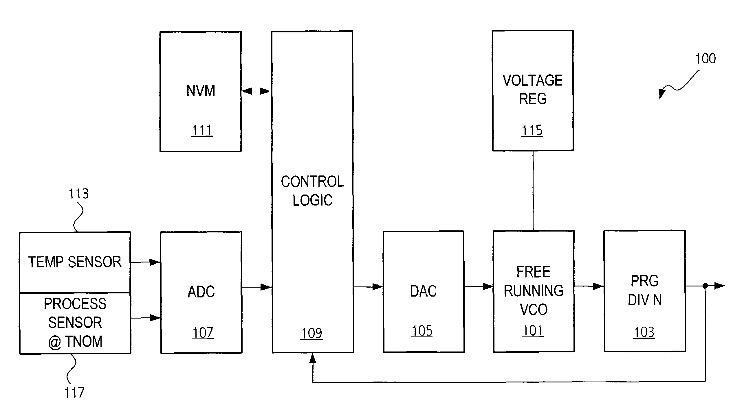
[0015]There are a large number of applications utilizing clock chips for which an accuracy of ±100 ppm is sufficient. Described herein is an architecture to build a clock chip, without using a reference source such as a crystal or surface acoustic wave (SAW) oscillator, that can achieve suitable accuracy on a fully integrated silicon solution, without the requirement for hermetic packaging and that can be manufactured at a very low cost. In one preferred embodiment, the die size is small (e.g., 2). A preferred embodiment may also include low pin counts and be compatible with existing crystal oscillator packages and pin-outs. For example, in an embodiment the integrated circuit may have VDD, GND, XOUT and ENABLE pins, where VDD and GND are power and ground, respectively, XOUT is the clock out signal and ENABLE enables the clock out signal. Note that term “pin” is used to generically refer to any sort of connection provided between the integrated circuit and an external signal. Other...
PUM
 Abstract
Description
Claims
Application Information
 - R&D
- Intellectual Property
- Life Sciences
- Materials
- Tech Scout
- Unparalleled Data Quality
- Higher Quality Content
- 60% Fewer Hallucinations
Browse by: Latest US Patents, China's latest patents, Technical Efficacy Thesaurus, Application Domain, Technology Topic, Popular Technical Reports.
© 2025 PatSnap. All rights reserved.Legal|Privacy policy|Modern Slavery Act Transparency Statement|Sitemap|About US| Contact US: help@patsnap.com


