Two F-number, two-color sensor system
a sensor system and f-number technology, applied in the field of two f-number, two-color sensor system, can solve the problems of significant increase in the cost of the sensor system, difficult to compare the two images by digital analysis techniques, etc., and achieve the effect of improving the quality of the image associated with the longer wavelength band, simple fabrication, and keeping in alignmen
- Summary
- Abstract
- Description
- Claims
- Application Information
AI Technical Summary
Benefits of technology
Problems solved by technology
Method used
Image
Examples
first embodiment
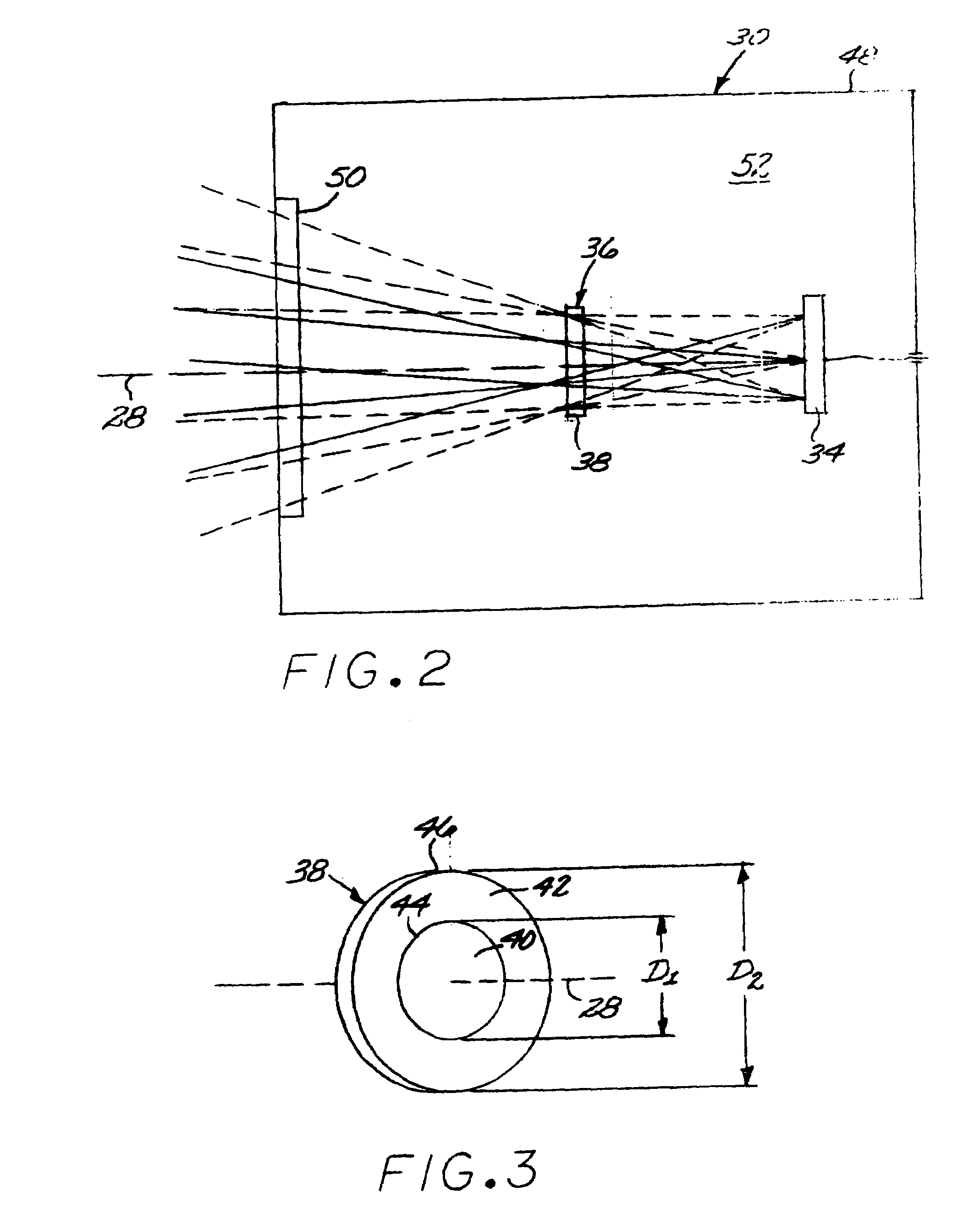
[0028]FIGS. 4 and 5 illustrate manufacturing sequences for two different embodiments of the structures of the cold-shield filter 38. In FIGS. 4A-E, the cold-shield filter 38 comprises a substrate 60 (FIG. 4A) having a first substrate portion 62 corresponding to the first filter portion 40 and a second substrate portion 64 corresponding to the second filter portion 42 (FIG. 4B). A first multilayer bandpass coating 66 is deposited to overlie the first substrate portion 62 (FIG. 4B), and a second multilayer bandpass coating 68 overlies the second substrate portion 64 (FIG. 4C). The bandpass filters may be designed to pass only a specific range of wavelengths, or they may be designed as edge filters to pass all light above or below a certain edge wavelength. The multilayer bandpass coatings 66 and 68 are multilayer structures designed to pass only certain wavelengths of light and to reflect or absorb other wavelengths of light. Such multilayer bandpass coatings are known in the art for ...
second embodiment
[0031]FIGS. 5A-5E depict a sequence for fabricating this The substrate 60 is first provided, FIG. 5A. The substrate 60 is etched to remove a portion of the thickness thereof in the second substrate portion 64, FIG. 5B. The second multilayer bandpass coating 68 is deposited overlying the second substrate portion 64, FIG. 5C. Optionally, the antireflection coating 70 is deposited, FIG. 5D, and the optical corrector is affixed or deposited, FIG. 5E. The antireflection coating 70, where used, is deposited over the unetched first substrate portion 62 and the second multilayer bandpass coating 68. For this reason, the depth of the etching in FIG. 5B is preferably exactly the optical thickness of the second multilayer bandpass coating 68, so that the antireflection coating 70 may be deposited upon a substantially flat surface.
PUM
 Abstract
Description
Claims
Application Information
 - R&D
- Intellectual Property
- Life Sciences
- Materials
- Tech Scout
- Unparalleled Data Quality
- Higher Quality Content
- 60% Fewer Hallucinations
Browse by: Latest US Patents, China's latest patents, Technical Efficacy Thesaurus, Application Domain, Technology Topic, Popular Technical Reports.
© 2025 PatSnap. All rights reserved.Legal|Privacy policy|Modern Slavery Act Transparency Statement|Sitemap|About US| Contact US: help@patsnap.com


