
Storage device for a multibus architecture

a storage device and bus technology, applied in the direction of static storage, program control, instruments, etc., can solve the problems of memory/bus connection, more complex multi-port memory and expensive implementation, and so as to prevent data loss or drop-out periods.

Inactive Publication Date: 2007-10-23
MICRONAS
View PDF14 Cites 5 Cited by
  • Summary
  • Abstract
  • Description
  • Claims
  • Application Information

AI Technical Summary

Benefits of technology

"The present invention relates to a storage device for a multibus architecture, which includes a memory and a switching device to connect the memory to different buses within the architecture. The storage device has an address analyzer to analyze the addresses on the buses and assign memory access for analysis. The switching device selectively connects the memory to one of the buses for memory access. The memory has an interrupt line to transmit interrupt signals to the processor, which controls the operation of the storage system. The storage system may have a plurality of memories connected to the multibus architecture, and the memories may be controlled alternately by the clock cycle. The use of memories in a processor is advantageous, and the invention also includes an adjustable separator device to assign any addresses and a logic device to output a block loss signal. The invention allows for efficient distribution of data between multiple memories and prevents loss of data or drop-out periods during switching operations between read and write states."

Problems solved by technology

Where these systems involve one or multiple data memories and multiple buses (i.e., a multibus architecture), the actual memory / bus connection is usually achieved in a manner which is relatively disadvantageous.
The first approach has the disadvantage that a multi-port memory is more complex and expensive to implement than a single-port memory.
The second approach has the disadvantage that separation of the memory blocks negatively affects program flexibility and execution speed.

Method used


Image

  • Storage device for a multibus architecture
  • Storage device for a multibus architecture
  • Storage device for a multibus architecture

Examples


Embodiment Construction

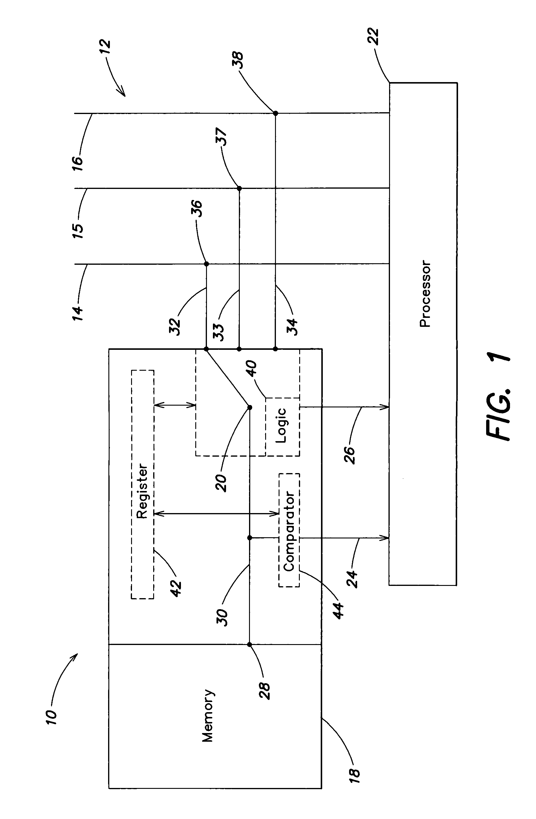
[0022]Referring to FIG. 1, a storage device 10 is connected to a multibus architecture 12, which may include three buses 14-16. The storage device 10 includes a memory 18 which may be selectively connected through a switching device 20 to one of the buses 14-16. Any additional components that might be required to operate the storage device 10, such as address buses and other control buses, may be added in accordance with the commonly available technical knowledge.

[0023]The memory 18 is connected through the multibus architecture 12 to a processor 22 according to the preferred embodiment. The processor 22 may have a storage system that includes a plurality of the memories 18, of which one bus 14-16 each is able to be controlled simultaneously for a memory access. As used herein, memory access means both the writing to the memory 18 of data (e.g., information data), and the reading of this data from a memory area of the memory 18 through one of buses 14-16. The buses 14-16 connect to ...


PUM


Abstract

A storage device for a multibus architecture includes at least one memory to store data, information, and / or addresses, along with a memory connection having a port to connect the memory to one of the buses of the multibus architecture. The memory connection, the port, and the bus have data lines to transmit data along with address lines to transmit addresses, and / or control information to control the memory and other devices connected to each specific bus within the multibus architecture. A switching device selectively connects the memory connection to one of the buses to enable a memory access to transmit data, addresses, and / or control information to or from the selected one of these buses.

Description

BACKGROUND OF THE INVENTION[0001]The invention relates in general to a multiple bus architecture associated with a signal processor and in particular to a memory storage device for use with such a multibus architecture.[0002]To achieve a relatively high throughput of data in signal processors, these processors often include multiple connected read / write buses through which a single data memory storage device may be accessed simultaneously. Control of memory addresses is typically implemented through read / write buses by alternately transmitting addresses and data, or by transmitting addresses through a separate address bus apart from a data bus.[0003]Where these systems involve one or multiple data memories and multiple buses (i.e., a multibus architecture), the actual memory / bus connection is usually achieved in a manner which is relatively disadvantageous. Two approaches are commonly utilized to achieve relatively efficient memory access to store data in the memory or to read data ...

Claims


Application Information

Patent Timeline
Patent Type & Authority Patents(United States)
IPC IPC(8): G06F12/00G11C7/10
CPCG11C7/1006
Inventor HERZ, RALFNOESKE, CARSTEN
Owner MICRONAS
Learn More