Methods and systems for achieving improved intellectual property protection for programmable logic devices

a programmable logic and intellectual property technology, applied in the field of intellectual property protection technologies, can solve the problems of significant capacity and complecity, inability to achieve similar development, and inability to achieve intellectual property protection embedded in such devices, such as programming patterns, to achieve the effect of improving intellectual property protection

Inactive Publication Date: 2007-06-26
ALTERA CORP
View PDF3 Cites 18 Cited by
  • Summary
  • Abstract
  • Description
  • Claims
  • Application Information

AI Technical Summary

Problems solved by technology

These devices have grown significantly in capability and complecity.
Yet intellectual property (IP) protection embedded in such devices, such as the programming patterns, has not enjoyed similar development.
The drawback of this IP protection scheme is that it relies on a decryption key 160, which must be stored somewhere on the chip.
As a result, this IP protection scheme is vulnerable to attack because it is not difficult for an attacker to reverse engineer the chip to obtain the decryption key.
In addition to being vulnerable to reverse engineering, storing a key on the chip may add production cost and complexity to chip manufacturers.

Method used


Image

  • Methods and systems for achieving improved intellectual property protection for programmable logic devices
  • Methods and systems for achieving improved intellectual property protection for programmable logic devices
  • Methods and systems for achieving improved intellectual property protection for programmable logic devices

Examples


Embodiment Construction

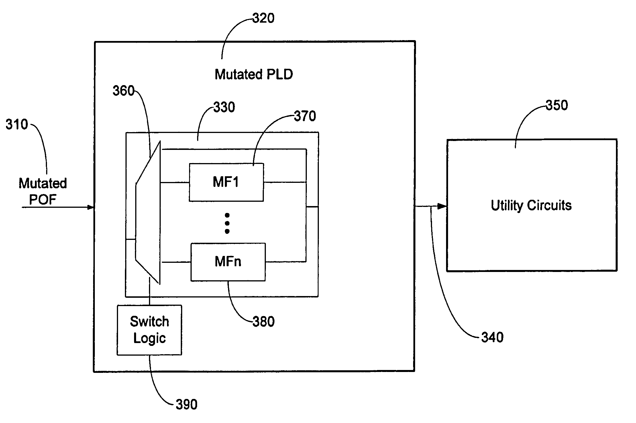
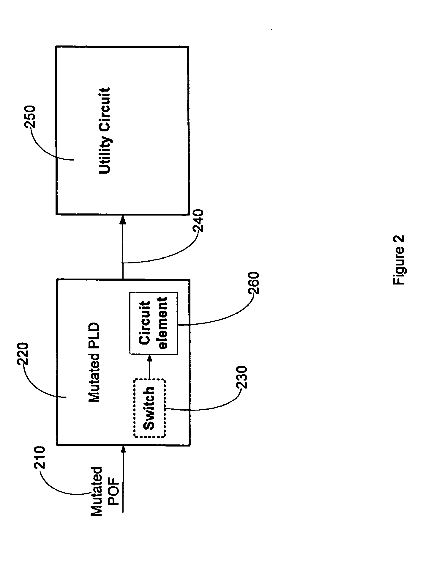
[0014]FIG. 2 shows one embodiment of the present invention. The system of FIG. 2 comprises a mutated PLD 220 programmed by a mutated programming pattern, or mutated POF 120. An output 240 of PLD 220 is applied to a utility circuit 250, which is intended to represent any circuit that might be connected to the output of a PLD. The mutated POF 210 is a POF that causes the mutated PLD 220 to generate a “mutated” output signal that causes the utility circuit 250 to function abnormally. The mutated POF 210 may be produced, for example, by altering a portion of the source code of a normal POF. The mutated PLD 220 also contains an additional circuit element 260. The additional circuit element 260 is capable of translating the mutated output signal to a normal output signal. Optionally, the system of FIG. 2 also contains a switch 230 for enabling or disabling the circuit element 260.

[0015]The system of FIG. 2 may be part of a system on a programmable chip (SOPC) using a PLD, such as a FPGA o...


PUM


Abstract

Methods and system for achieving improved copyright protection for programmable logic devices are disclosed. One preferred embodiment comprises a programmable logic device comprising a programmable element programmed by a mutated programming pattern, said mutated programming pattern causing the PLD to generate a mutated output; and a circuit element that translates the mutated output into a normal output.

Description

FIELD OF INVENTION[0001]This invention is related in general to intellectual property protection technologies and in particular to methods and systems for achieving improved intellectual property protection for programmable logic devices.BACKGROUND OF INVENTION[0002]Programmable logic devices (PLD) such as field programmable gate arrays (FPGA) and complex programmable logic devices (CPLD) are digital logic circuits that can be programmed by certain “programming patterns” such as programmable object files (POFs) to perform logical functions. These devices have grown significantly in capability and complecity. Yet intellectual property (IP) protection embedded in such devices, such as the programming patterns, has not enjoyed similar development.[0003]Currently, most IP protection schemes rely on encrypting / decrypting the programming patterns on chip. FIG. 1 shows a typical encryption / decryption IP protection scheme that includes a decrypter 120 that receives an encrypted POF 110 and ...

Claims


Application Information

Patent Timeline
IPC IPC(8): H03K19/177G06F12/14
CPCH03K19/17732H03K19/17768
Inventor CHANG, RICHARD Y.
Owner ALTERA CORP
Why Eureka
Try Eureka