Method for mapping a logic circuit to a programmable look up table (LUT)

a logic circuit and look up table technology, applied in the field of programmable gate arrays, can solve the problems of reduced computation time, inability to apply all designs, and too expensive approaches, etc., and achieve the effect of reducing computation time taken

Inactive Publication Date: 2007-03-13
SICRONIC REMOTE KG LLC
View PDF5 Cites 0 Cited by
  • Summary
  • Abstract
  • Description
  • Claims
  • Application Information

AI Technical Summary

Benefits of technology

[0013]An object of this invention is to overcome the above drawbacks in the prior art and provide a method for LUT based mapping for reducing computation time taken and providing a near depth optimal mapping approach.

Problems solved by technology

However, most of these approaches result in either local optimal or exponential time complexity.
Hence, these approaches are too expensive and cannot be applied for all designs.
Such reduction techniques do not give an optimal solution or even a near optimal solution.
The Flow-diagram process described above suffers from a drawback, that the runtime of the process gets increased while constructing sub-networks and finding a cut for each node of the circuit.
This increase becomes even more prominent when the delay of a circuit increases.

Method used


Image

  • Method for mapping a logic circuit to a programmable look up table (LUT)
  • Method for mapping a logic circuit to a programmable look up table (LUT)
  • Method for mapping a logic circuit to a programmable look up table (LUT)

Examples


Embodiment Construction

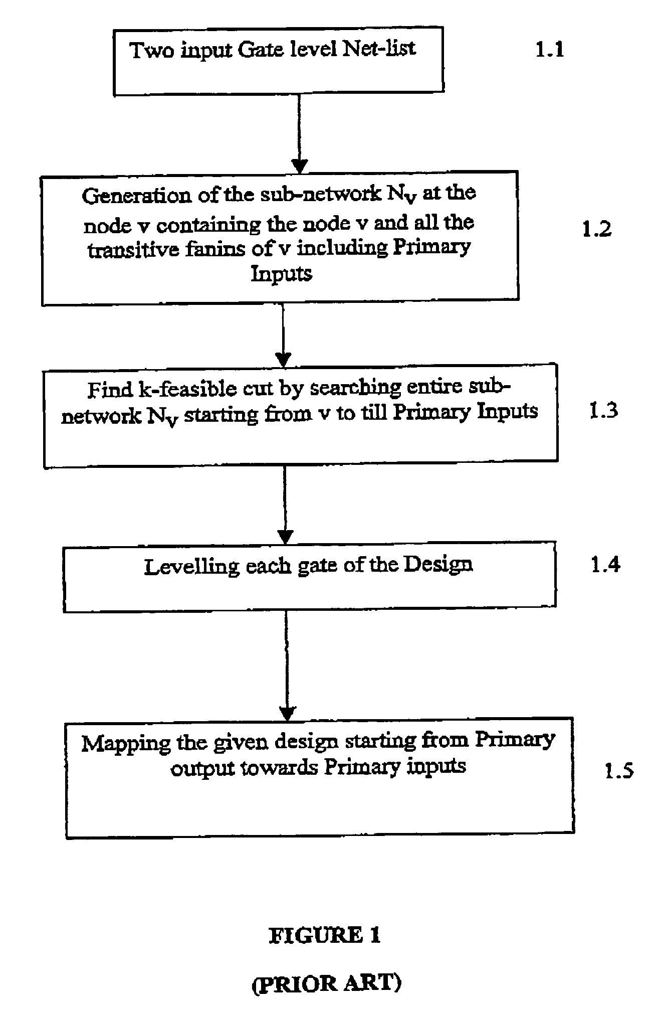
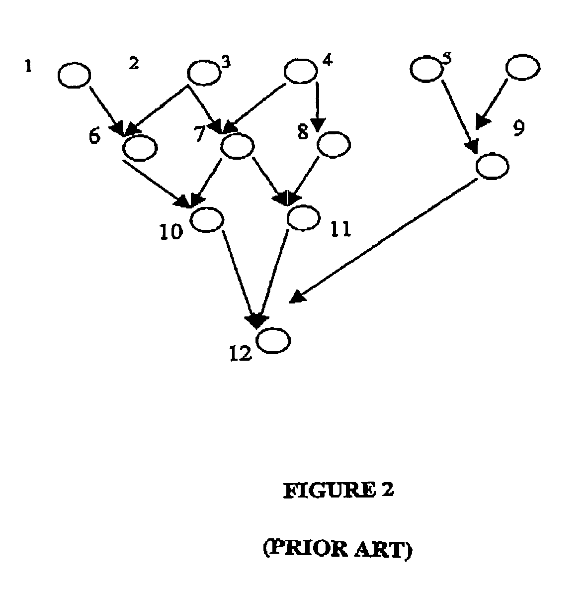
[0021]FIG. 1, and FIG. 2 have already been described in the background of the invention.

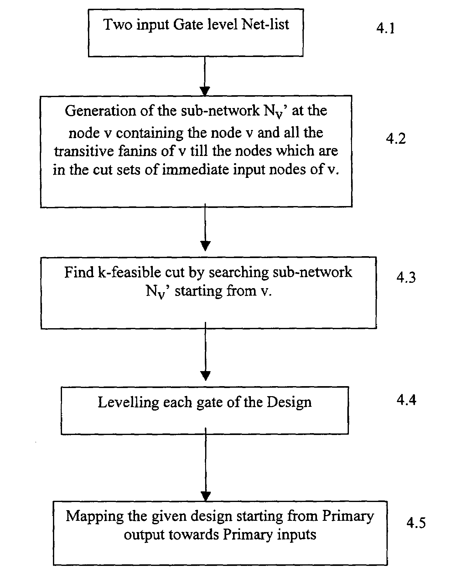
[0022]FIG. 3 shows the process / algorithm depicting the steps provided by the present invention for LUT mapping. First, the gate level Net-list is input for providing information about the logic gates to be mapped 4.1. The next step 4.2 is the generation of the sub-network Nt(v) at node v containing the node v itself along with all the transitive fanins of v until the nodes which are in the cut sets of immediate input nodes of v. This step is an improvement over the conventional mapping methods as it significantly reduces the number of nodes to be considered for mapping each time a new node is to be mapped. Further, in step 4.3 the k-feasible cut is found out for the sub-network Nt(v) by searching the sub-network starting from node v.

[0023]In the present method for constructing sub-network Nt(v) for each node v of the network N, let v1 be a node for which all fanins are primary inputs. Sub-network...


PUM


Abstract

The method for mapping a logic circuit to a plurality of interconnectable, programmable look up tables (LUT) elements includes forming logic element groups including individual logic elements and / or previously formed logic element groups that are capable of being accommodated within the fanin and / or fanout capacity of a target LUT. The method further includes mapping the formed logic element group to the target LUT, and repeating the process for forming logic element groups and mapping to target LUTs for the entire network in a manner such that at each stage only the unmapped logic element / elements and mapped logic element groups of the previous stage are considered for mapping.

Description

FIELD OF THE INVENTION[0001]The present invention relates to Field Programmable Gate Arrays (FPGA), and, more particularly, to methods for mapping a logic circuit to a programmable look up table.BACKGROUND OF THE INVENTION[0002]A programmable logic array device has a plurality of logic elements connected through an interconnect architecture. Electrical circuits are mapped over these logic elements to allow the device to perform desired operations. Mapping of an electrical circuit to an FPGA is a time consuming process, and thus it is desired to increase the speed of the mapping process.[0003]The important objectives during mapping of an electrical circuit over an FPGA are, to map the maximum number of circuit elements over a single logic element and to achieve the smallest possible tree of logic elements to realize the electrical circuit. Different technologies propose different methods for achieving these objectives. For example, R. J. Francis et al. in “Chortle-crf: Fast Technolog...

Claims


Application Information

Patent Timeline
Patent Type & Authority Patents(United States)
IPC IPC(8): G06F17/50H03K19/00
CPCG06F17/5054G06F30/34
Inventor SHARMA, SUNIL KUMARTOMAR, AJAYSAMANTA, DHABALENDU
Owner SICRONIC REMOTE KG LLC
Why Eureka
Try Eureka