Semiconductor laser device containing laser driver and electronic equipment having the same

a laser device and semiconductor technology, applied in semiconductor lasers, semiconductor laser structure details, optical beam sources, etc., can solve the problems of insufficient thinning and cost reduction of equipment using laser devices, and the inability to achieve the downsizing of laser devices alone, even if achieved, to achieve the effect of reducing the cost of electronic equipment, and reducing the size of the laser devi

Inactive Publication Date: 2007-02-27
SHARP KK
View PDF11 Cites 2 Cited by
  • Summary
  • Abstract
  • Description
  • Claims
  • Application Information

AI Technical Summary

Benefits of technology

The present invention provides a semiconductor laser device containing a laser driver that can be further downsized, thinned, and cost-reduced. The device includes a semiconductor laser element and a laser driver mounted on a common mount surface and accommodated in a common package. The device also includes a signal detection part for performing photoelectric conversion. The laser driver and signal detection part can be placed on both sides of the semiconductor laser element to reduce heat influence and improve signal detection. The laser driver and signal detection part can be integrated as a submount member, reducing parts count and assembly working man-hours. The technical effects of the invention include further downsizing, thinning, and cost-reduction of the semiconductor laser device containing a laser driver.

Problems solved by technology

As a result of this, there has been a problem that downsizing, thinning and cost reduction of equipment using the laser device cannot be implemented sufficiently.
In other words, since the laser device and the laser driver are generally used in combination, downsizing of the laser device alone, even if accomplished, could not produce so much effect.

Method used


Image

  • Semiconductor laser device containing laser driver and electronic equipment having the same
  • Semiconductor laser device containing laser driver and electronic equipment having the same
  • Semiconductor laser device containing laser driver and electronic equipment having the same

Examples


first embodiment

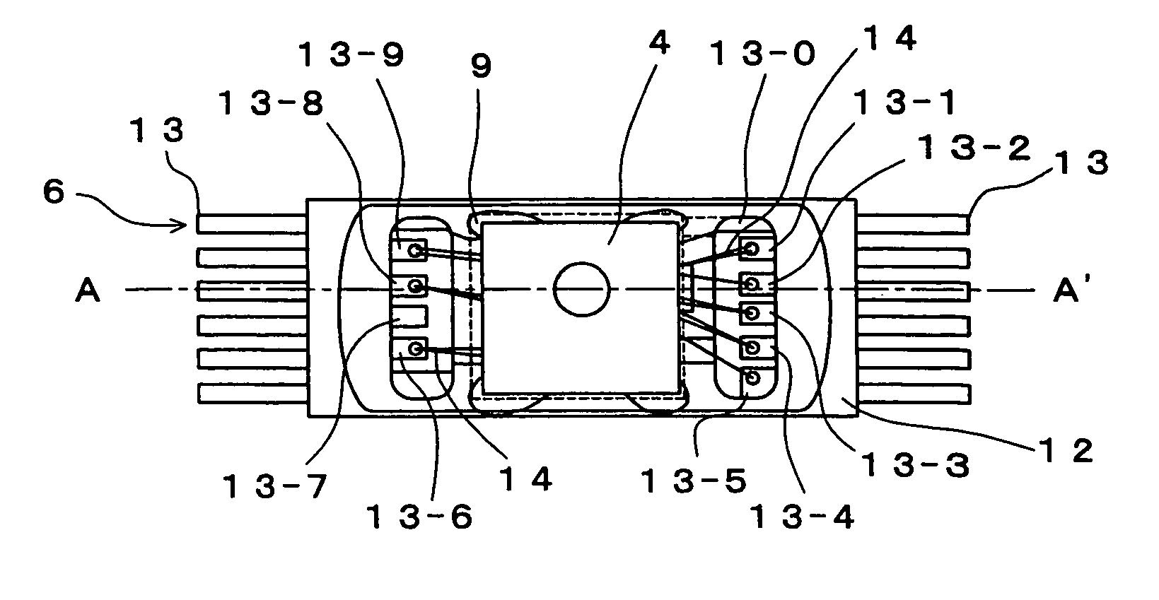
[0065]FIG. 1A shows the semiconductor laser device containing a laser driver according to the invention as viewed from above, and FIG. 1B schematically shows an A–A′ cross section in FIG. 1A.

[0066]This semiconductor laser device containing a laser driver is equipped with a lead frame 6, and a resin package 12 integrally formed with a resin mold so that a mount portion 60 of this lead frame 6 is surrounded by the resin package 12. The package 12 has an opening at its upper portion 12a.

[0067]The lead frame 6 includes a mount portion (also referred to as island or die-pad) 60 having a flat, rectangular mount surface 60a, and lead pins 13, 13, . . . extending from vicinities of the mount portion 60 toward both sides of the A–A′ direction (rightward and leftward directions in FIG. 1) within a plane along the mount surface 60a. It is noted that reference numerals 13-0, 13-1, . . . , 13-9 denote inner lead portions present within the package 12 out of the lead pins 13, 13, . . . .

[0068]On...

second embodiment

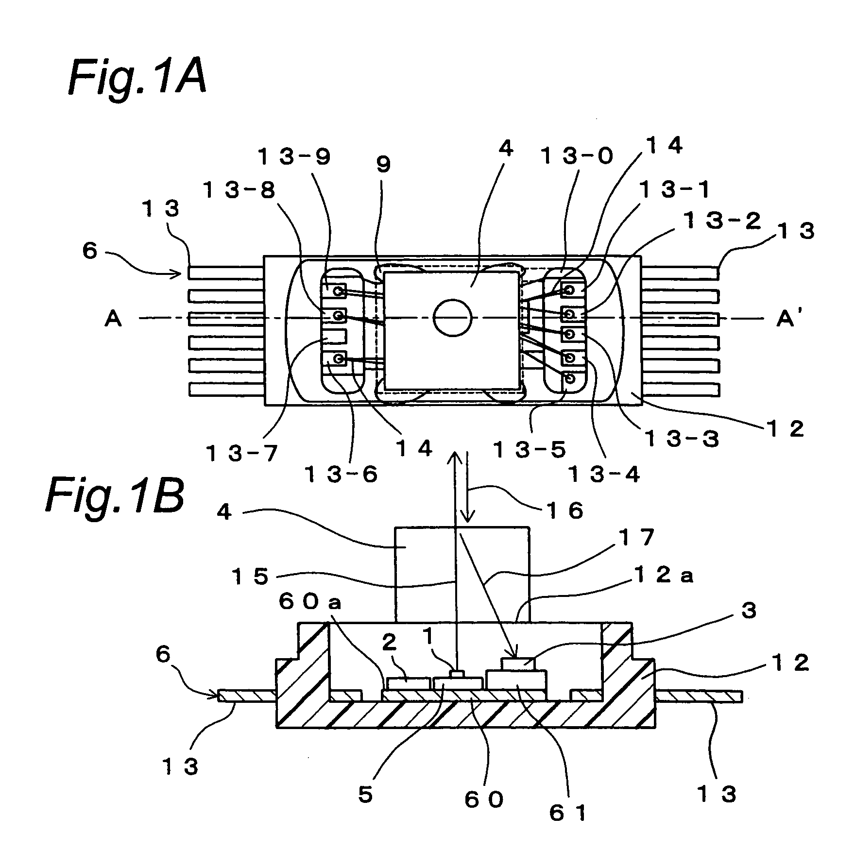
[0076]FIG. 2A shows a semiconductor laser device containing a laser driver as viewed from above, and FIG. 2B schematically shows an A–A′ cross section in FIG. 2A. It is noted that the same constituent members as those in FIGS. 1A and 1B are designated by like reference numerals and their overlapped description is omitted (applicable also hereinafter).

[0077]In this semiconductor laser device containing a laser driver, the laser driver 2 and the signal detection part 3 are disposed on both sides with respect to the optical axis of the semiconductor laser element 1 (i.e., at both-side positions of an optical axis on a plane containing the optical axis) and moreover in such a direction that the laser light 15 emitted by the semiconductor laser element 1 results in a narrower breadth 10. In this example, the laser driver 2, the semiconductor laser element 1 and the signal detection part 3 are disposed so as to be arrayed in this order along the A–A′ direction as in the first embodiment....

third embodiment

[0079]FIG. 3A shows a semiconductor laser device containing a laser driver as viewed from above, and FIG. 3B schematically shows an A–A′ cross section in FIG. 3A.

[0080]In this semiconductor laser device containing a laser driver, a monitor detection part for monitoring an optical output of the semiconductor laser element 1, and a laser driver for driving the semiconductor laser element 1 based on an output of this monitor detection part, are integrated as a submount member 7 having a planar outer configuration. Then, this submount member 7 is disposed between the semiconductor laser element 1 and the mount surface 60a so as to be vertical to the optical axis of the semiconductor laser element 1. The other constituent members are similar in construction to those of the first embodiment.

[0081]In this semiconductor laser device containing a laser driver, since the semiconductor laser element 1, the submount member 7 including the monitor detection part and the laser driver, and the si...


PUM

PropertyMeasurementUnit
optical outputaaaaaaaaaa
opticalaaaaaaaaaa
heataaaaaaaaaa

Abstract

There is provided a semiconductor laser device containing a laser driver capable of implementing downsizing, thinning and cost reduction of equipment using the laser device. In the semiconductor laser device containing a laser driver, a semiconductor laser element, a laser driver for driving the laser element, and a signal detection part for performing photoelectric conversion are mounted on a common mount surface of a lead frame and moreover accommodated in a common package. Upward of the semiconductor laser element is provided a hologram element for transmitting laser light emitted by the laser element toward a recording medium and then diffracting toward the signal detection part the laser light reflected by the recording medium. The laser driver and the signal detection part are disposed on both sides with respect to an optical axis of the laser element.

Description

BACKGROUND OF THE INVENTION[0001]The present invention relates to a semiconductor laser device containing a laser driver. More particularly, the invention relates to a semiconductor laser device in which a semiconductor laser element as well as a laser driver for driving the laser element are mounted on a lead frame.[0002]Also, the present invention relates to electronic equipment having such a semiconductor laser device containing a laser driver.[0003]Conventionally, there has been known a semiconductor laser device as shown in FIGS. 9A and 9B (see FIG. 4 of Japanese Patent Laid-Open Publication HEI 6-203403). This semiconductor laser device is fabricated through the steps of forming a resin package 112 with a resin mold so that a mount portion 160 of a lead frame 106 is surrounded by the resin package 112, die-bonding on the mount portion a planar submount 105 on which a mirror (not shown) and a semiconductor laser element 101 are mounted, further die-bonding on a submount 161 the...

Claims


Application Information

Patent Timeline
Patent Type & Authority Patents(United States)
IPC IPC(8): H01S5/00G11B7/125G11B7/135H01S3/04H01S5/02H01S5/022H01S5/024H01S5/0683
CPCH01S5/02216H01S5/005H01S5/02H01L2224/48137H01S5/02292H01S5/024H01S5/0683H01S5/02248H01S5/02325H01S5/02255
Inventor TAKEMORI, HIROTOSHI
Owner SHARP KK
Why Eureka
Try Eureka