Efficient asynchronous stuffing insertion and destuffing removal circuit

Active Publication Date: 2007-02-20
MACOM CONNECTIVITY SOLUTIONS LLC
View PDF17 Cites 14 Cited by
  • Summary
  • Abstract
  • Description
  • Claims
  • Application Information

AI Technical Summary

Benefits of technology

[0010]In accordance with the present invention, a digital communications system is provided that can asynchronously map / de-map digital signals from one clock domain to another, while reducing mapping jitter levels and permitting higher levels of integration. In one embodiment, the digital communications system comprises an asynchronous stuff bit insertion circuit, an asynchronous stuff bit removal circuit, and a communications network connected between the asynchronous stuff bit insertion and removal circuits. The asynchronous stuff bit insertion circuit is configured for asynchronously mapping one or more data frames from a first clock domain to the clock domain of the network. Further, the asynchronous stuff bit removal circuit is configured for asynchronously de-mapping the data frames from the clock domain of the network to the first clock domain.
[0011]In the presently disclosed embodiment, the asynchronous stuff bit insertion circuit includes a first elastic store, and a barrel shifter coupled to the first elastic store. The first elastic store operates as a temporary gross data frame storage, while the barrel shifter operates as a temporary fine data frame storage. The first elastic store is configured to receive a predetermined number of bytes of each data frame at a time. The first elastic store is further configured for temporarily storing a predetermined number of data words, each word having a width equal to the predetermined number of data frame bytes received by the elastic store. The barrel shifter is configured for successively receiving the predetermined number of data frame bytes from the first elastic store, and successively providing the predetermined number of data frame bytes to a stuffing circuit, which is communicatively connected to the communications network. Read and write pointers associated with the barrel shifter are periodically monitored, and in the event the read pointer is within a specified number of locations from the write pointer, the first elastic store is directed to provide the predetermined number of data frame bytes to the barrel shifter. The stuffing circuit is configured to make stuffing decisions based on the periodic measurements of the time delay through the first elastic store and the barrel shifter. In this way, data frames can be asynchronously mapped from the first clock domain to the clock domain of the network.
[0012]The asynchronous stuff bit removal circuit includes a de-stuffing circuit for receiving the data frame bytes from the communications network, a first divider circuit coupled to the de-stuffing circuit, a second divider circuit, a second elastic store coupled between the first and second divider circuits, and a frequency control path connecting respective clock inputs of the first and second divider circuits. The clock inputs of the de-stuffing circuit and the first divider circuit are in the clock domain of the network, and the clock input of the second divider circuit is in the above-described first clock domain. The frequency control path includes a phase-locked loop having a variable divider circuit, the operation of which is controlled based on the presence / absence of stuff bits in the data frame bytes provided to the de-stuffing circuit by the network. The asynchronous stuff bit removal circuit is configured for de-stuffing the data frame bytes, and re-covering the clock signal of the first clock domain. In this way, data frames can be asynchronously de-mapped from the clock domain of the communications network to the first clock domain.
[0013]By employing the first elastic store for temporary gross data frame storage and the barrel shifter for temporary fine data frame storage to reduce the number of gates in the asynchronous stuff bit insertion circuit, integration levels are increased. Further, by employing the frequency control path in the asynchronous stuff bit removal circuit to recover the clock signal of the first clock domain, mapping jitter levels in the digital communications system are reduced.

Problems solved by technology

One drawback of the above-described timing compensation mechanism is that sufficient resolution often cannot be achieved using the FIFO buffer.
However, performing de-stuffing and stuffing operations at such a relatively low byte resolution can unduly complicate the asynchronous mapping of the data frames.
In addition, variations in the instantaneous rate of the data frames caused by the interspersing of the stuff bits frequently causes mapping jitter to be introduced into the communications system.
However, the timing compensation mechanism including the circular buffer also has drawbacks.
Further, a significant amount of control logic would typically be required to control the shifting of the data frame bytes through the 512-byte circular buffer.
This can be problematic when implementing the circular buffer on an Application Specific Integrated Circuit (ASIC) because such an implementation would normally entail the use of a relatively large number of custom gates, which can increase the die size and lead to increased manufacturing costs.
In addition, like the timing compensation mechanism that includes the FIFO buffer, the mechanism including the circular buffer frequently causes mapping jitter to be introduced into the communications system.

Method used


Image

  • Efficient asynchronous stuffing insertion and destuffing removal circuit
  • Efficient asynchronous stuffing insertion and destuffing removal circuit
  • Efficient asynchronous stuffing insertion and destuffing removal circuit

Examples


Embodiment Construction

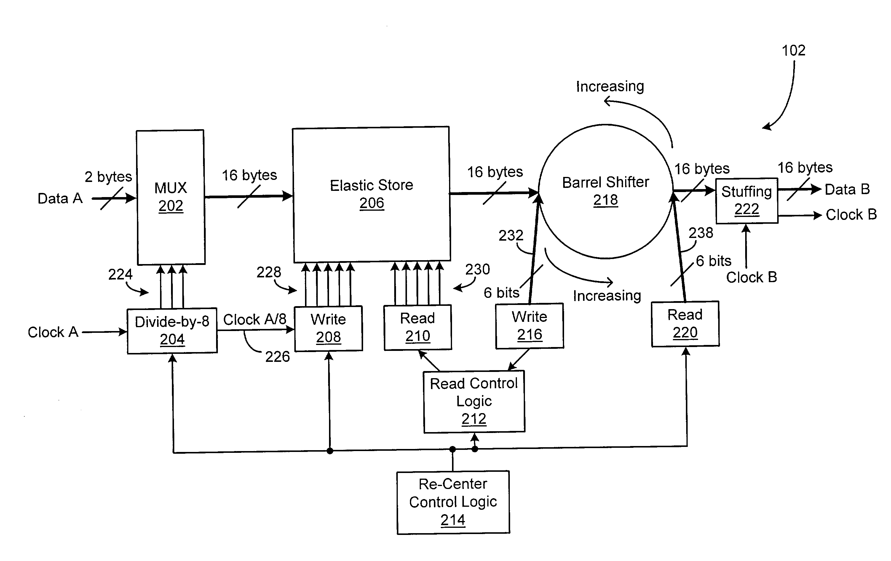
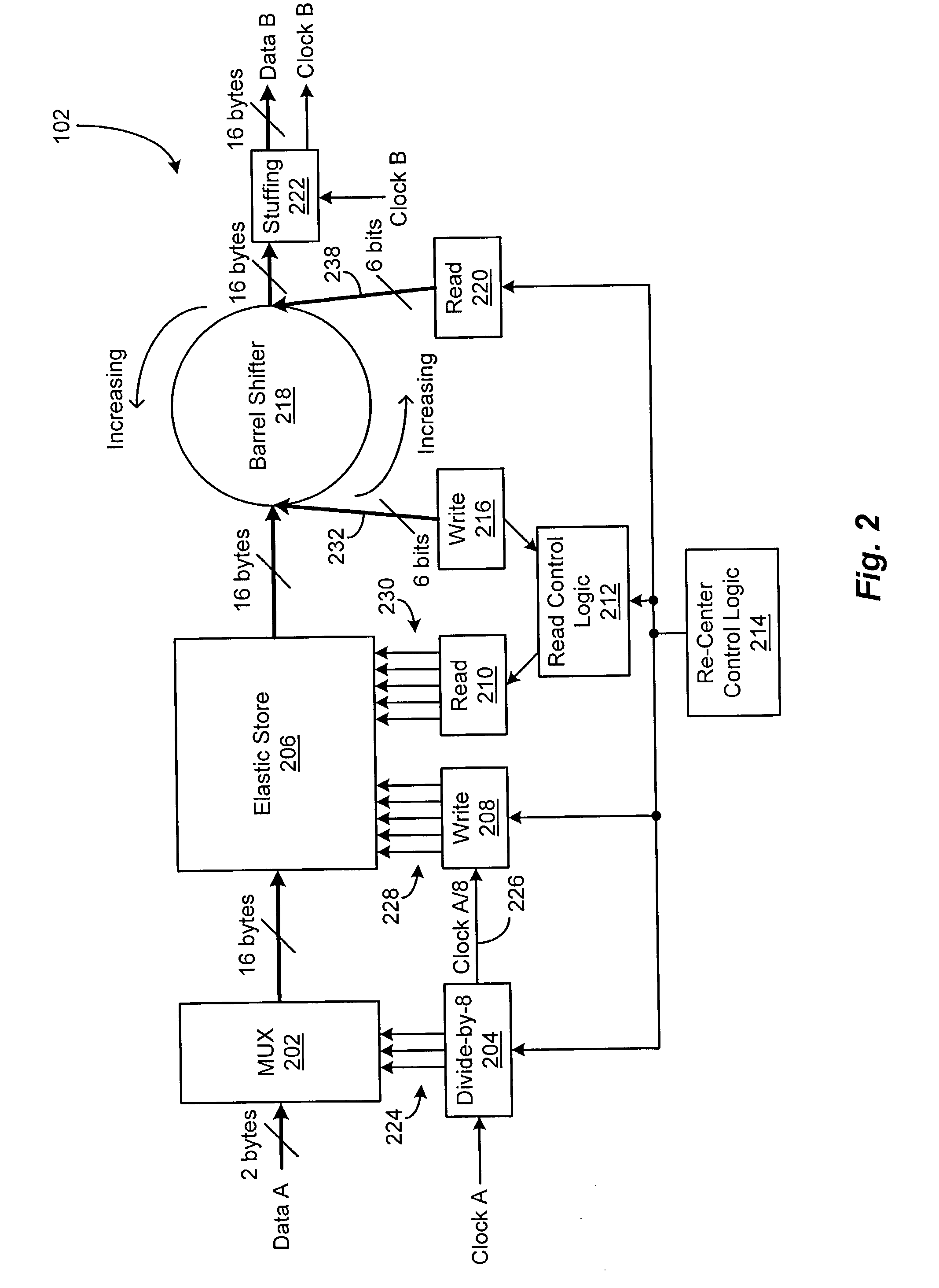
[0021]A digital communications system is disclosed that has the capability of asynchronously mapping / de-mapping digital signals from one clock domain to another. In the presently disclosed system, the asynchronous mapping capability is provided by an asynchronous stuff bit insertion circuit, which includes an elastic store for temporary gross data frame storage and a barrel shifter for temporary fine data frame storage. Use of the elastic store in combination with the barrel shifter allows increased levels of integration in the asynchronous stuff bit insertion circuit. Further, the asynchronous de-mapping capability is provided by an asynchronous stuff bit removal circuit, which includes a frequency control path that allows mapping jitter levels in the system to be reduced.

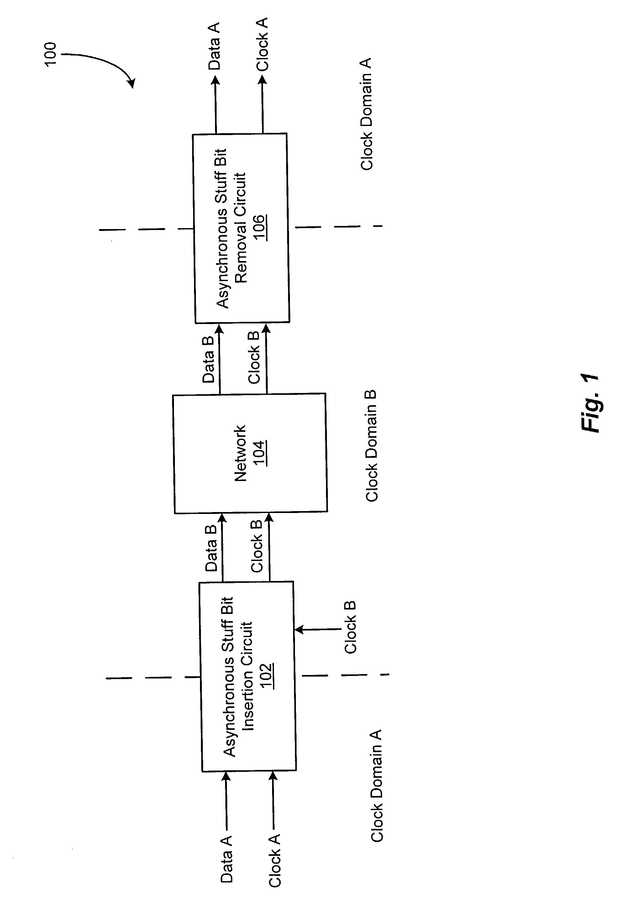
[0022]FIG. 1 depicts an illustrative embodiment of a digital communications system 100, in accordance with the present invention. In the illustrated embodiment, the digital communications system 100 includes an as...


PUM


Abstract

A digital communications system that can asynchronously map / de-map digital signals from one clock domain to another, while reducing mapping jitter levels and permitting higher levels of integration. The digital communications system includes an asynchronous stuff bit insertion circuit, an asynchronous stuff bit removal circuit, and a communications network connected therebetween. The asynchronous stuff bit insertion circuit includes a first elastic store, a barrel shifter, and a stuffing circuit. The asynchronous stuff bit removal circuit includes a de-stuffing circuit, a second elastic store, and a frequency control path including a phase-locked loop having a variable divider circuit, the operation of which is controlled based on the presence / absence of stuff bits in the data provided to the de-stuffing circuit. By employing the first elastic store for temporary gross data frame storage and the barrel shifter for temporary fine data frame storage to reduce the number of gates in the asynchronous stuff bit insertion circuit, integration levels are increased. Further, by employing the frequency control path in the asynchronous stuff bit removal circuit to recover the clock signal of the first clock domain, mapping jitter levels in the digital communications system are reduced.

Description

CROSS REFERENCE TO RELATED APPLICATIONS[0001]N / ASTATEMENT REGARDING FEDERALLY SPONSORED RESEARCH OR DEVELOPMENT[0002]N / ABACKGROUND OF THE INVENTION[0003]The present invention relates generally to digital communications systems, and more specifically to digital communications systems in which digital signals are asynchronously mapped / de-mapped from one clock domain to another.[0004]Digital communications systems are known that can transport one or more digital signals, e.g., data frames, across multiple clock domains. A conventional digital communications system having such a capability includes a first communications network operating at a first clock rate connected to a second communications network operating at a second clock rate, in which the first clock signal is asynchronous to the second clock signal. The conventional digital communications system further includes a mechanism configured to compensate for the timing differences between the first and second clock signals when t...

Claims


Application Information

Patent Timeline
IPC IPC(8): H04J3/07H04J3/06H04L7/00H04Q11/04
CPCH04J3/073H04J2203/0089
Inventor WALKER, TIMOTHY P.QUIRK, JAYCAMPEAU, SEAN
Owner MACOM CONNECTIVITY SOLUTIONS LLC
Why Eureka
Try Eureka