High emission low voltage electron emitter
a low-voltage electron and high-emitting technology, applied in the field of electron emitters, can solve the problems of low energy required for electron emission, high panel fabrication cost, complex panel fabrication process,
- Summary
- Abstract
- Description
- Claims
- Application Information
AI Technical Summary
Benefits of technology
Problems solved by technology
Method used
Image

Examples
first embodiment
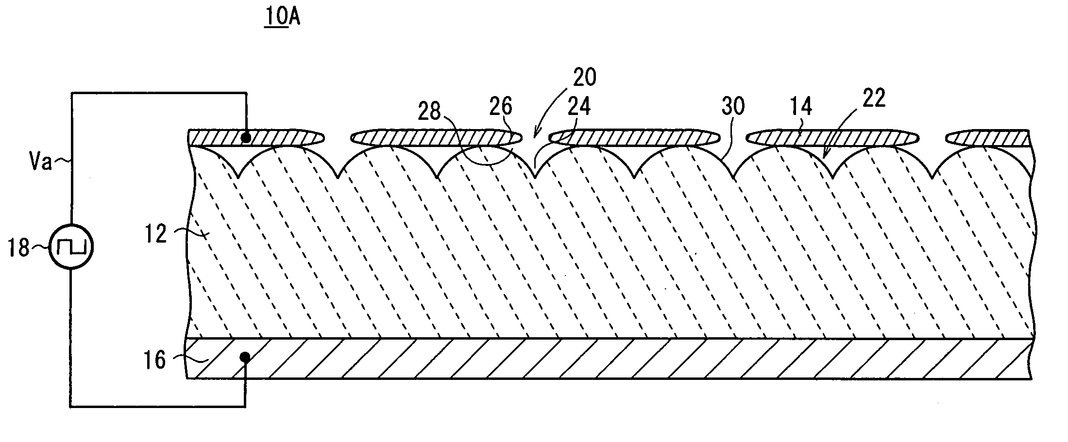
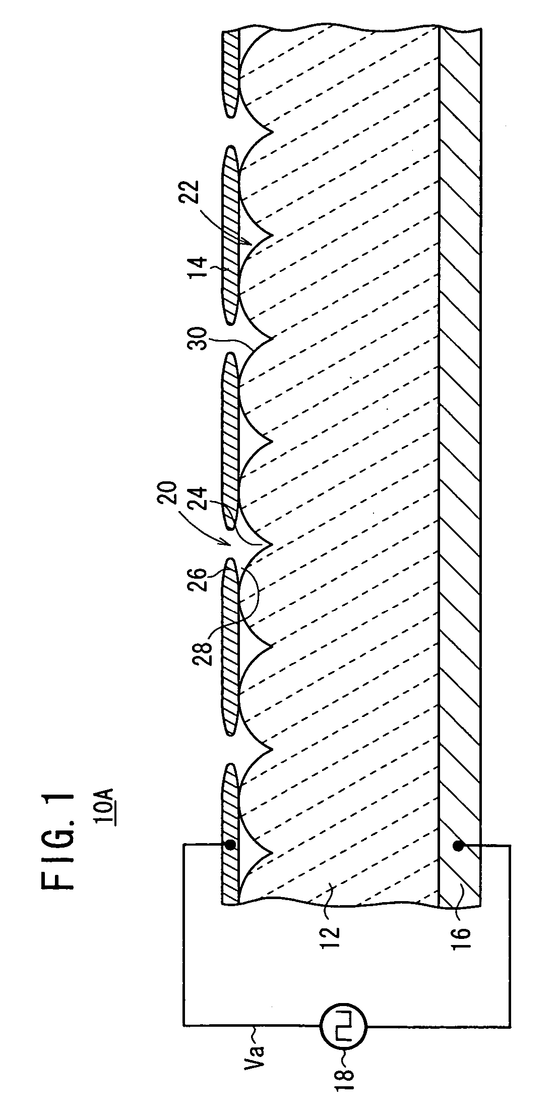
[0119]As shown in FIG. 1, an electron emitter 10A comprises a plate-like emitter (a substance serving as an emitter) 12 made of a dielectric material, a first electrode (e.g., an upper electrode) 14 formed on a first surface (e.g., an upper surface) of the emitter 12, a second electrode (e.g., a lower electrode) 16 formed on a second surface (e.g., a lower surface) of the emitter 12, and a pulse generation source 18 for applying a drive voltage Va between the upper electrode 14 and the lower electrode 16.
[0120]The upper electrode 14 has a plurality of through regions 20 where the emitter 12 is exposed. The emitter 12 has surface irregularities 22 due to the grain boundary of the dielectric material. The through regions 20 of the upper electrode 14 are formed in areas corresponding to concavities 24 due to the grain boundary of the dielectric material. In the embodiment shown in FIG. 1, one through region 20 is formed in association with one recess 24. However, one through region 20...
second embodiment
[0251]An electron emitter 10B will be described below with reference to FIG. 33.
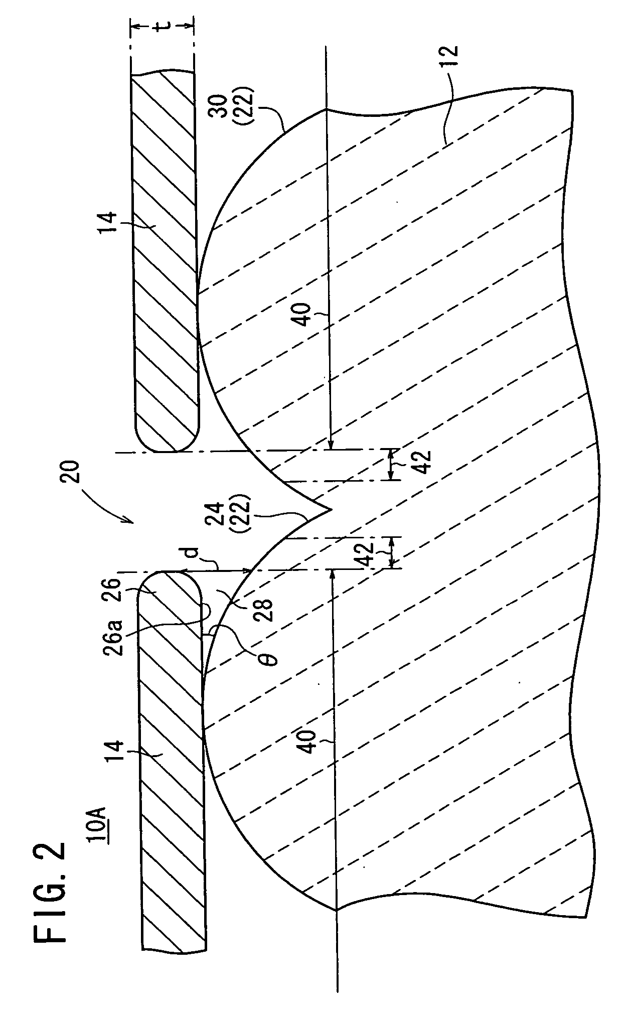
[0252]As shown in FIG. 33, the electron emitter 10B according to the second embodiment is of an arrangement that is essentially the same as the electron emitter 10A according to the first embodiment, but is characterized in that the upper electrode 14 has a thickness t greater than 40 μm, and the through region 20 is artificially formed by etching (wet etching or dry etching), liftoff, laser, etc. The through region 20 may be shaped as the hole 32, the recess 44, or the slit 48.
[0253]The lower surface 26a of the peripheral portion 26 of the through region 20 in the upper electrode 14 is inclined progressively upwardly toward the center of the through region 20. This shape may simply be formed by liftoff, for example.
[0254]The electron emitter 10B according to the second embodiment is capable of easily producing a high electric field concentration as with the electron emitter 10A according to the first e...
third embodiment
[0258]An electron emitter 10C will be described below with reference to FIG. 37.
[0259]As shown in FIG. 37, the electron emitter 10C is of an arrangement that is essentially the same as the electron emitter 10A according to the first embodiment, but differs therefrom in that it has one board 60 made of ceramics, a lower electrode 16 formed on the board 60, an emitter 12 formed on the board 60 in covering relation to the lower electrode 16, and an upper electrode 14 formed on the emitter 12.
[0260]The board 60 has a cavity 62 defined in the position corresponding to each emitter 12 and serving part of a thin-wall portion. The cavity 62 communicates with the exterior via a small-diameter through hole 64 which is defined in the opposite end surface of the board 60.
[0261]The board 60 includes a thin-wall portion lying over the cavity 62 (hereinafter referred to as “thin-wall portion 66”) and a thick-wall portion other than the thin-wall portion, which functions as a stationary block 68 s...
PUM
 Abstract
Description
Claims
Application Information
 - R&D
- Intellectual Property
- Life Sciences
- Materials
- Tech Scout
- Unparalleled Data Quality
- Higher Quality Content
- 60% Fewer Hallucinations
Browse by: Latest US Patents, China's latest patents, Technical Efficacy Thesaurus, Application Domain, Technology Topic, Popular Technical Reports.
© 2025 PatSnap. All rights reserved.Legal|Privacy policy|Modern Slavery Act Transparency Statement|Sitemap|About US| Contact US: help@patsnap.com