Integrated dual damascene RIE process with organic patterning layer

a dual-damascene, organic technology, applied in the manufacturing of semiconductor/solid-state devices, basic electric elements, electric devices, etc., can solve the problems of increasing the damage to the exposed dielectric, imposing the burden of requiring a greater total processing time for dual-damascene formation, and insufficient remaining thickness of the remaining layer to withstand the duration of the ild etching step, etc., to achieve the effect of reducing the stripping time for the trench

Inactive Publication Date: 2006-10-31
GLOBALFOUNDRIES INC
View PDF6 Cites 22 Cited by
  • Summary
  • Abstract
  • Description
  • Claims
  • Application Information

AI Technical Summary

Benefits of technology

[0007]Combining the above process into the integrated via / trench process described herein reduces the stripping time for the trench and via. During a “via first” process the vias are formed and the resist is stripped. Next a planarizing layer of organic polymer (photoresist like material) is applied filling the vias and forming a flat planar layer over the ILD. A resist layer and an ARC layer are applied and the step of trench etching is carried out. The trench pattern is transferred into the low k ILD through the excess planarizing layer and into the low k ILD. When the trenches are etched to the correct depth the excess organic material in the bottom portion of the via needs to be stripped out along with any remaining resist, so the via sees 2× strip.

Problems solved by technology

Furthermore, as it has been necessary to employ photolithography to print smaller features, tit has been necessary to thin the photoresist to a point at which the remaining thickness thereof is insufficient to withstand the duration of the ILD etching step while retaining the critical dimensions.
If one were to employ separate via and trench processing steps that would have the disadvantage of imposing the burden of requiring greater total processing time for dual-damascene formation.
In practice, in many cases dielectric materials, based on methyl substituted siloxanes are used, and the stripping process from the via and trench steps increases the damage to the exposed dielectric removing methylene groups near the surface of the dielectric layers and increasing the dielectric strength of the low k ILD layer.

Method used


Image

  • Integrated dual damascene RIE process with organic patterning layer
  • Integrated dual damascene RIE process with organic patterning layer
  • Integrated dual damascene RIE process with organic patterning layer

Examples


example 1

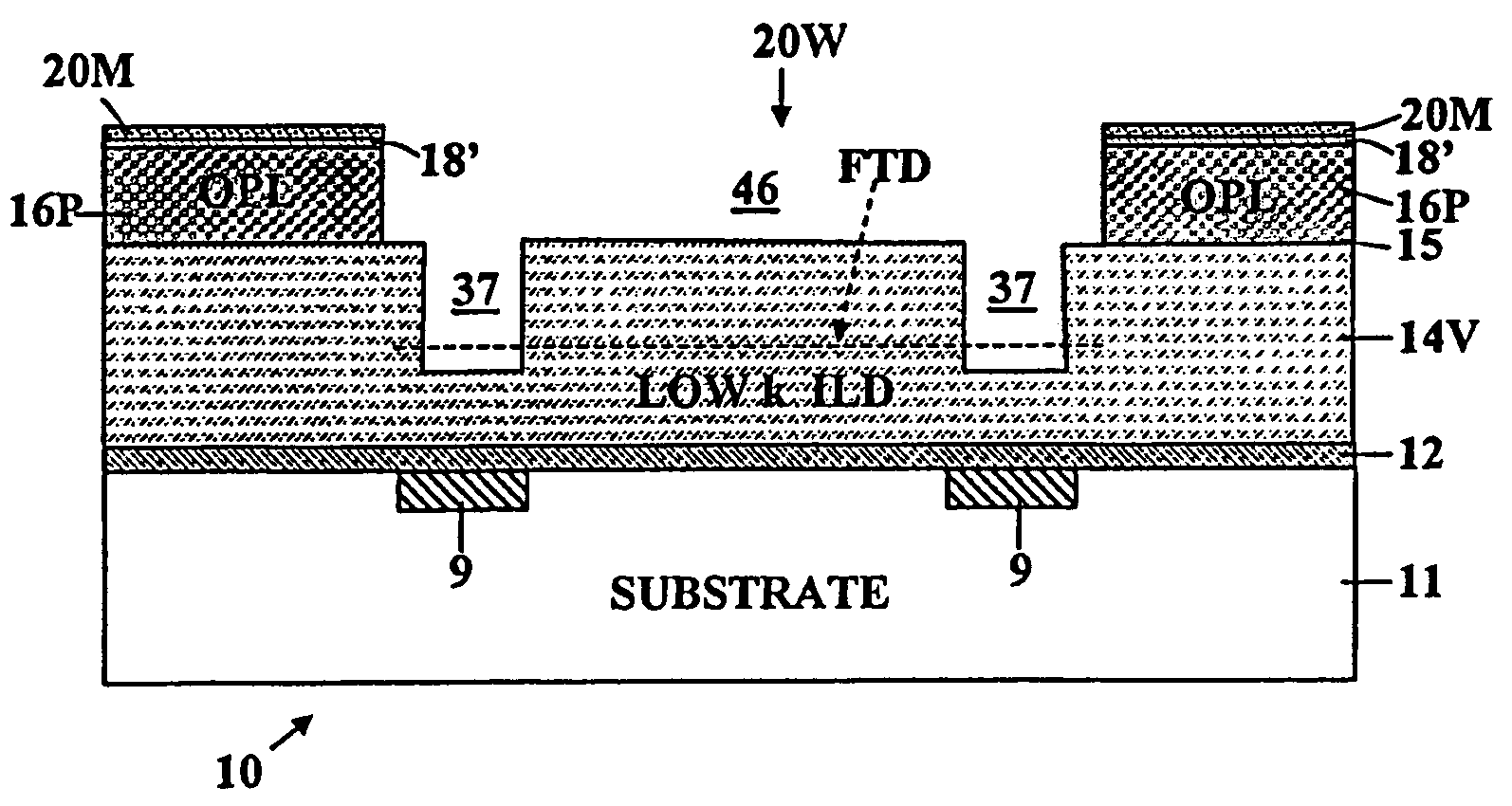
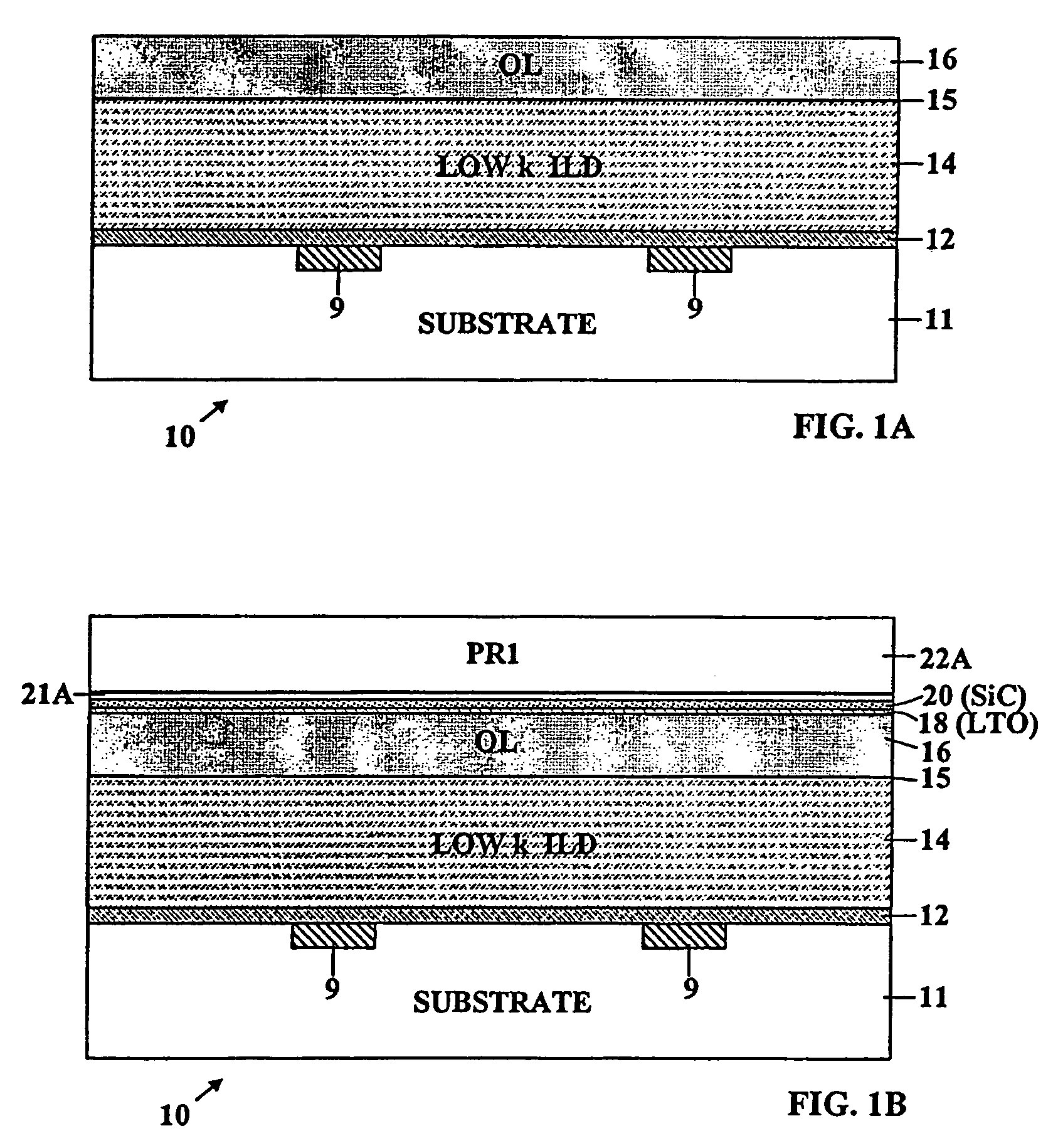
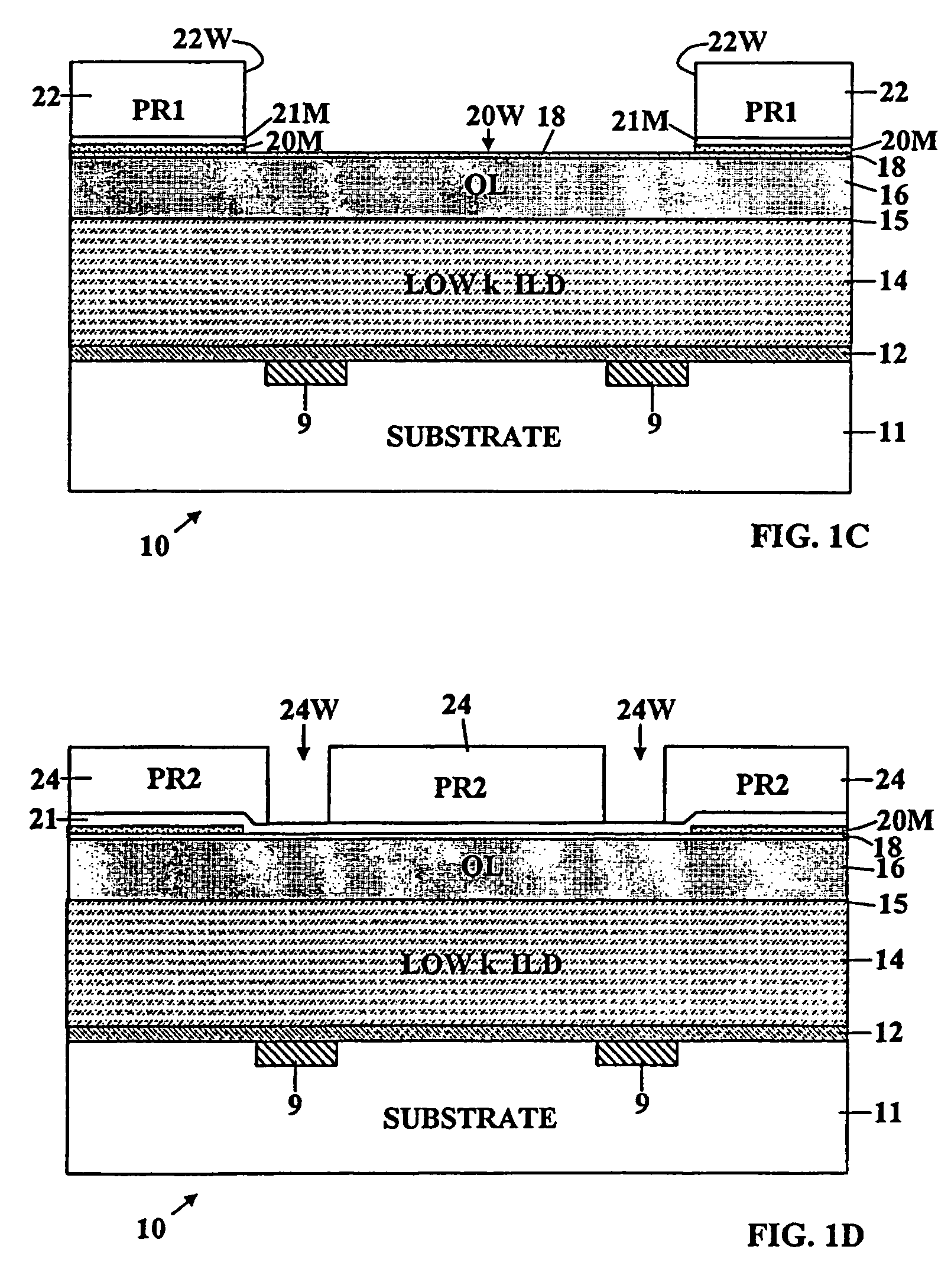
[0028]After the OL layer 16 is deposited, the lower, via hard mask layer 18 of a thickness of about 35 nm of silicon oxide is deposited thereover. Over the lower, via hard mask layer 18, a second, toy, trench hard mask layer 20 composed of Si3N4 of a thickness of about 30 nm is deposited. The photoresist mask 22A and ARC layer 21A for trench definition are applied and developed and a plasma etch is used to etch the Si3N4 top, trench hard mask layer 20 and stop on or in the silicon oxide lower, via hard mask layer 18. Plasma etch conditions for this selective etch include an RF (Radio Frequency) system operating at 27 MHz and 2 MHz in a parallel plate configuration. Operating pressure is in the range of 30 to 60 mTorr and gases include Ar, CHF3 or CH2F2, and CO with flows at 300 sccm, 30 sccm, 50 sccm and 200 sccm respectively. The amount of power applied to the electrodes is of the level of 350 watts and 100 watts for the 27 MHz and for the 2 MHz frequencies, respectively. Typical e...

example 2

[0029]After the OL layer 16 is deposited a lower hard mask layer 18 of a thickness of about 15 nm of silicon carbide is deposited. Over this layer the top hard mask layer 20 of Si3N4 of a thickness of about 30 nm is deposited. The photoresist 20A and ARC 21A for trench definition are applied and developed and plasma etch is used to etch the Si3N4 of the top hard mask layer 20 and stop on or in the silicon oxide of the lower hard mask layer 18. Plasma etch conditions for this selective etch include an RF system operating at 27 MHz and 2 MHz in a parallel plate configuration. Operating pressure is in the range of 30 to 60 mTorr and gases include Ar, CF4 and CHF3 and O2 with flows at 300 sccm, 80 sccm, 30 sccm and 10 sccm respectively. The amount of power which is applied to the electrodes is of the level of 500 watts and 100 watts for the 27 MHz and for the 2 MHz frequencies, respectively. Typical etch times are short and are of the order of less than 50 seconds. The transition of the...


PUM


Abstract

A dual damascene conductor structure is formed on a substrate with an exposed conductor on top covered by a buried cap, a dielectric layer (DL) and an organic layer (OL). Form a lower via hard mask layers over the OL and form a top trench patterning hard mask over the lower, via hard mask. Form a trench pattern hole through the trench hard mask layer; and form a via pattern hole through the via hard mask layer in a region exposed below the trench pattern hole. Etch a via pattern hole into the OL and then etch a via pattern hole down into the DL. Etch away the trench pattern layer and the OL layer below the trench pattern hole. Etch the via hole through the DL exposing the cap while simultaneously partially etching the DL to a final trench depth to form a trench in the DL below the trench pattern hole, with the trench having a bottom above the cap and sidewalls in the DL.

Description

BACKGROUND OF THE INVENTION[0001]This invention relates to semiconductor devices and more particularly to methods of Form interconnections between conductors in such devices.[0002]As is well understood by those skilled in the art of manufacture of semiconductor devices photoresist masking layers are used for patterning vias and trenches by photolithography. As the Critical Dimensions (CDs) of vias and trenches for advanced semiconductor devices continue to become smaller and the photoresist masking layers used for patterning the vias and trenches become thinner. The thickness of an intermediate layer known as a low k Inter-Level Dielectric (ILD) layer may not scale down in proportion to the photoresist masking layers.[0003]A preferred method for manufacture of metal interconnects is to form a Damascene structure. Damascene wiring interconnects are formed by depositing an Inter-Layer Dielectric (ILD) layer on a planar surface. Then the ILD layer is patterned using lithography to form...

Claims


Application Information

Patent Timeline
Patent Type & Authority Patents(United States)
IPC IPC(8): H01L21/4763
CPCH01L21/31116H01L21/31138H01L21/31144H01L21/76811H01L21/76813
Inventor AMERICA, WILLIAM G.JOHNSTON, STEVEN H.
Owner GLOBALFOUNDRIES INC
Why Eureka
Try Eureka