
System and method for power gating

a power gating and system technology, applied in the field of power gating, can solve the problems of affecting reliability, circuit may latch the wrong value or switch at the wrong time, and ground bounce in neighboring circuits,

Inactive Publication Date: 2006-08-08
IBM CORP
View PDF8 Cites 23 Cited by
  • Summary
  • Abstract
  • Description
  • Claims
  • Application Information

AI Technical Summary

Benefits of technology

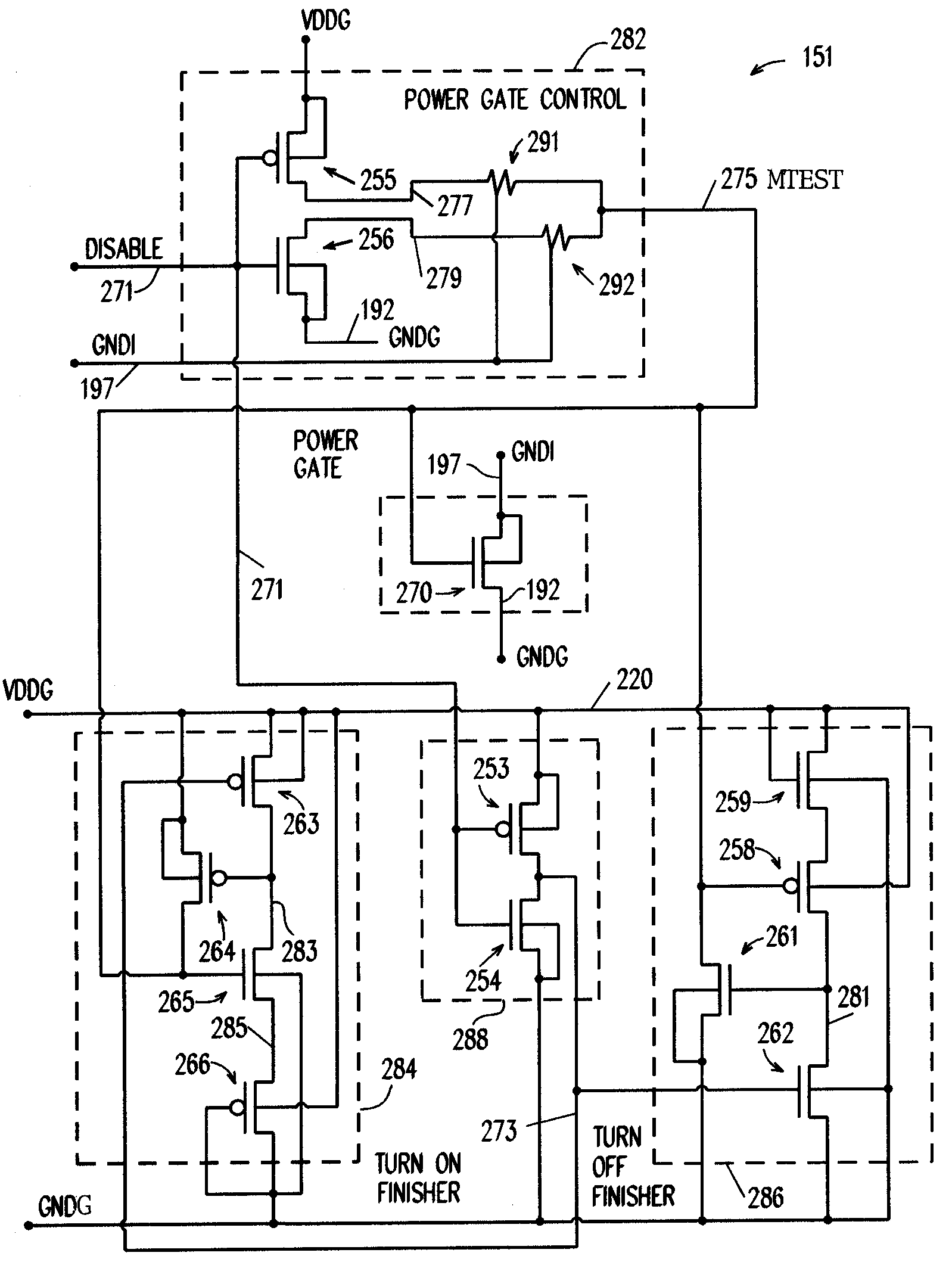
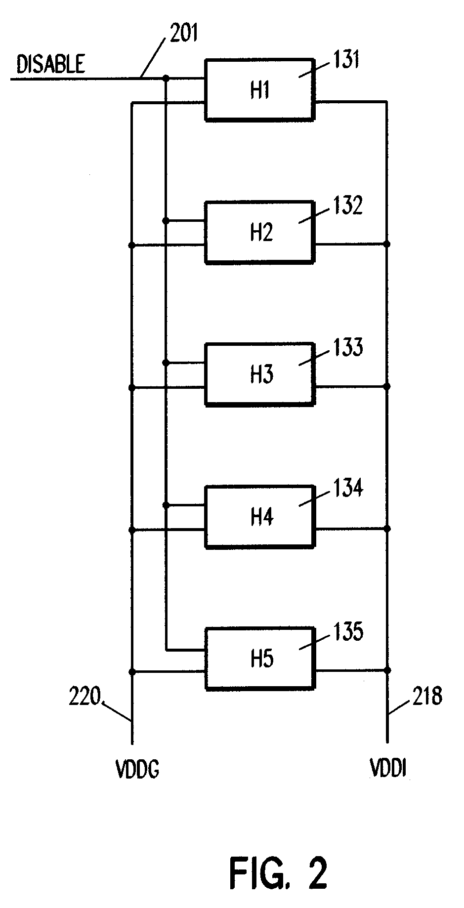
The patent describes a system and method for controlling power supply to a specific area of a circuit. This is done by using a global voltage to power the circuit, and then selectively shorting the global voltage to the specific area through a power gate controlled by a disable signal. The system also includes a control circuit and a test signal to turn off or on the power gate as needed. The technical effect of this invention is to provide a more efficient and controlled power supply to specific areas of a circuit, while managing noise and leakage.

Problems solved by technology

The patent text discusses the problem of leakage currents in CMOS technologies, which can cause issues in power-sensitive applications. To manage this, chip architectures have incorporated voltage islands, but this can lead to ground bounce, which affects the reliability of a system-on-a-chip. The text proposes using power gating to switch the power supplies of multiple islands, but this can create additional design challenges, such as current spikes and power supply noise. The technical problem is to address these challenges and improve the stability and performance of operational circuits on the chip.

Method used


Image

  • System and method for power gating
  • System and method for power gating
  • System and method for power gating

Examples


Embodiment Construction

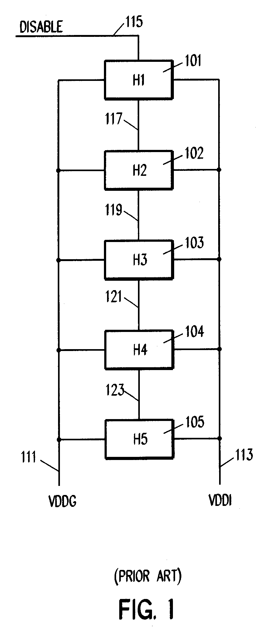
[0023]Referring to FIG. 1, by way of illustration of problems associated with prior solutions, five headers 101–105 are connected in parallel between the chip VDD 111 (VDDG) and the island VDD 113 (VDDI) for which they provide power gating. A single disable signal 15 is daisy chained, as is represented by lines 117, 119, 121, and 123, from header 101 to header 105. This architecture does not scale up particularly well for large numbers of headers. Since the number of headers typically increases in proportion to the area of an island, the turn-on and turn-off delay of such a gating scheme is a strong function of island size. Furthermore, since headers earlier in such a daisy-chain, such as headers 101 and 102, can turn on well before those late in the chain, such as headers 104 and 105, the earlier headers carry a large fraction of the current required to power up an island, which can lead to significant concentrations of current in the first headers in a chain and thus to ‘hot spots...


PUM


Abstract

Power is gated from global terrain to a voltage island while controlling leakage and managing transient power supply noise. The voltage island includes a field effect transistor (FET) power gate, a first connection to a global voltage source and a second connection to a disable signal source, and an island voltage net for supplying voltage to devices on the island. A power gate control circuit is responsive to the disable signal source for generating a test signal for selectively turning off the FET power gate as the disable signal source goes to a logical ‘1’, and for turning on the FET power gate as said disable source goes to a logical ‘0’. The FET power gate is responsive to the disable signal source being off for connecting the island voltage net to the global voltage source. A turn on finisher circuit is responsive to the disable signal transitioning to on and to the test signal for holding the power gate solidly on; and a turn off finisher circuit is responsive to the disable signal transitioning to off and to the test signal for holding said power gate solidly off.

Description


Claims


Application Information

Patent Timeline
Owner IBM CORP
Learn More