


Quick Research
Generate reliable direction feasibility study reports for your R&D in just a few steps.

Technical Q&A
Discover and master advanced knowledge NOW. Basics, ideas, possibilities, all at once.

Find Solutions
As an expert in R&D theories, this can generate solutions to your technical problems instantly.

Evaluate Feasibility
Analyze your overall solution with one click, know your potential R&D risks in advance.

Monitor Landscape
Get weekly tech updates, stay abreast of the latest tech innovations and key insights.
Electron and hole modulating electrodes in organic light emitting diodes
- Summary
- Abstract
- Description
- Claims
- Application Information
AI Technical Summary
Benefits of technology
Problems solved by technology
Method used
Image

Examples
Embodiment Construction
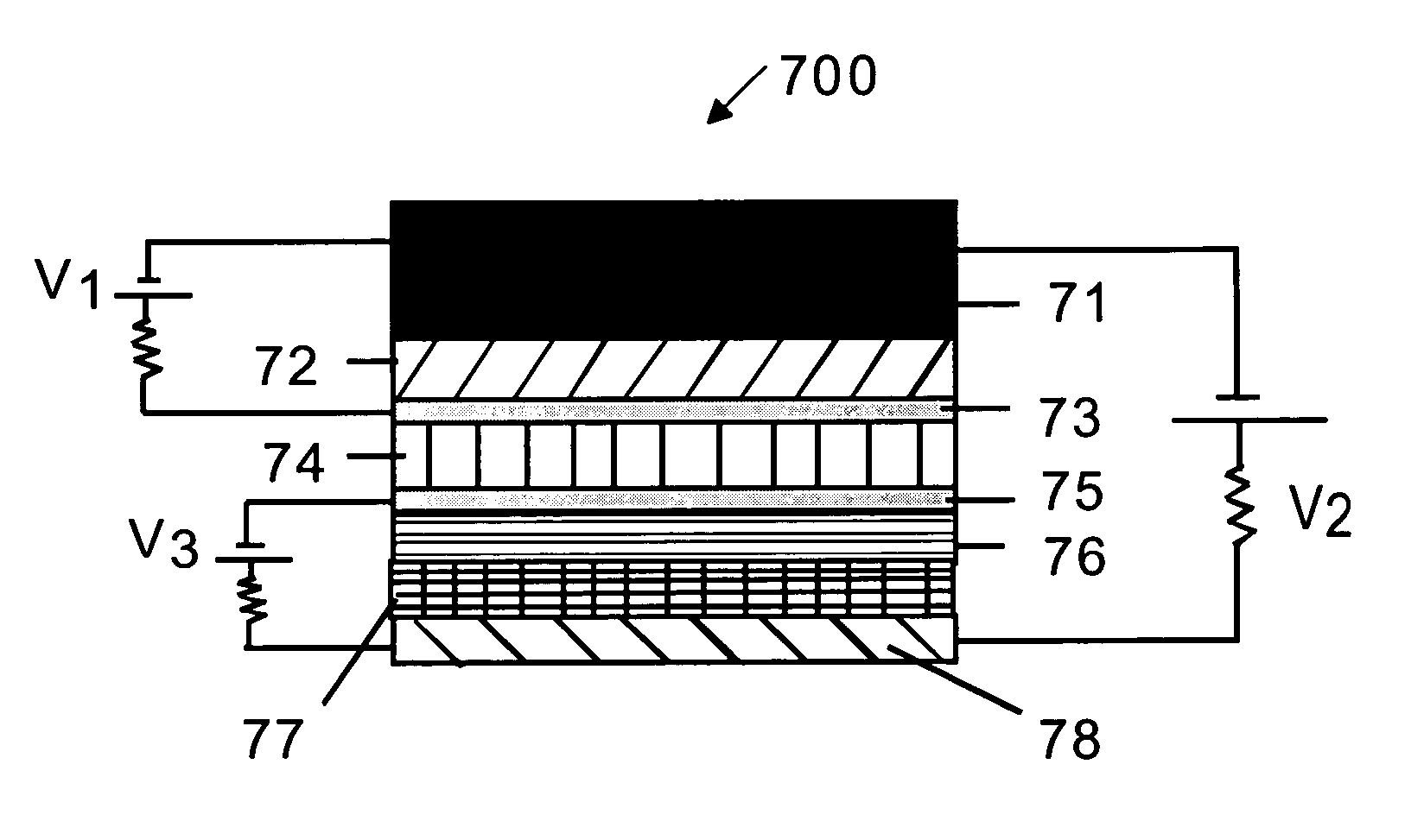
[0022]FIG. 1 depicts the cross-section of thin film layers in a conventional OLED structure 100 that is applied with a voltage V2 to emit light. A metallic cathode layer 1 is applied with a small negative voltage and a transparent anode layer 6, that is deposited usually on a glass substrate, not shown in FIG. 1, is applied with a small positive voltage. The organic layer 2 serves as electron transport layer for the electrons emitted from cathode layer 1. Similarly the organic layer 4 functions as hole-transport layer for the holes injected from the organic layer 5. The holes are injected from the anode layer 6, which is transparent in this embodiment. Layer 5 is called hole injection layer and the layer 4 is called hole transport layer. In certain configurations, layer 4 can perform the function of hole-injection and hole transport. When a voltage of sufficient magnitude V2 is applied to the cathode and anode, the holes and electrons are transported to the layer 3, which is called ...
PUM
 Abstract
Description
Claims
Application Information
 - R&D Engineer
- R&D Manager
- IP Professional
- Industry Leading Data Capabilities
- Powerful AI technology
- Patent DNA Extraction
Browse by: Latest US Patents, China's latest patents, Technical Efficacy Thesaurus, Application Domain, Technology Topic, Popular Technical Reports.
© 2024 PatSnap. All rights reserved.Legal|Privacy policy|Modern Slavery Act Transparency Statement|Sitemap|About US| Contact US: help@patsnap.com