
Semiconductor memory device for controlling cell block with state machine

a memory device and state machine technology, applied in the field of semiconductor memory devices, can solve the problems of slow operation speed of the memory device than the cpu, complicated circuit configuration of the controlling unit, and obstacle to high speed operation, and achieve the effect of facilitating driving control

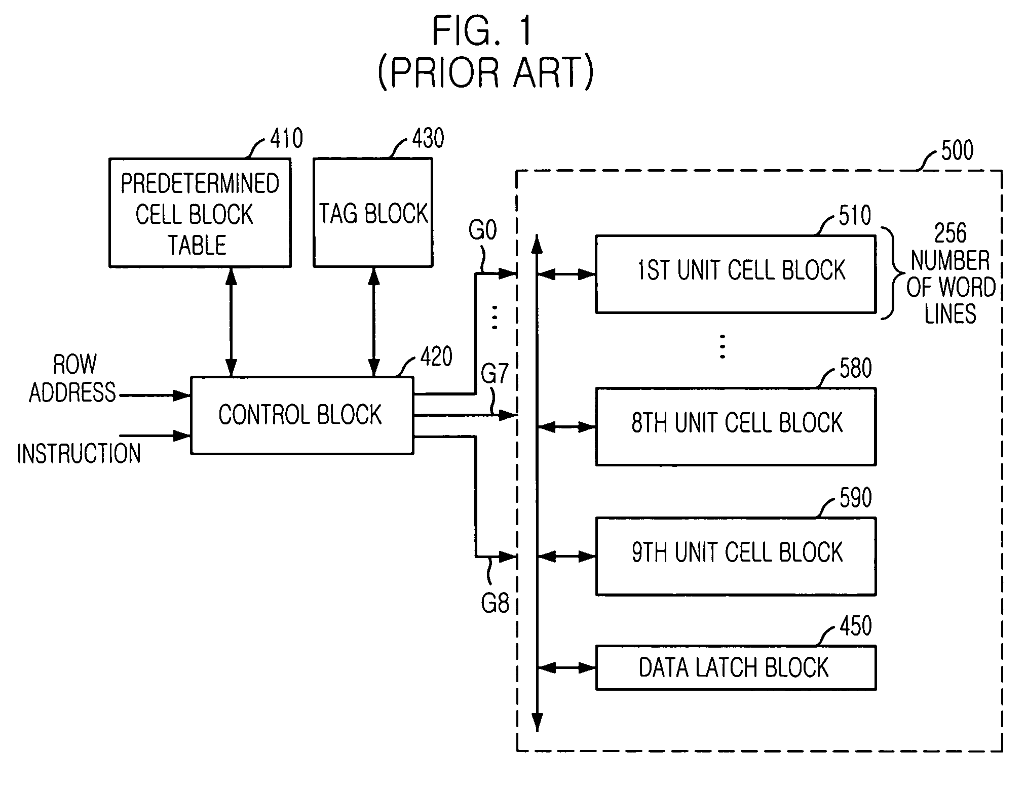
Inactive Publication Date: 2006-06-27
SK HYNIX INC
View PDF4 Cites 4 Cited by
  • Summary
  • Abstract
  • Description
  • Claims
  • Application Information

AI Technical Summary

Problems solved by technology

Such slower operational speed of the memory device than the CPU leads some problems.
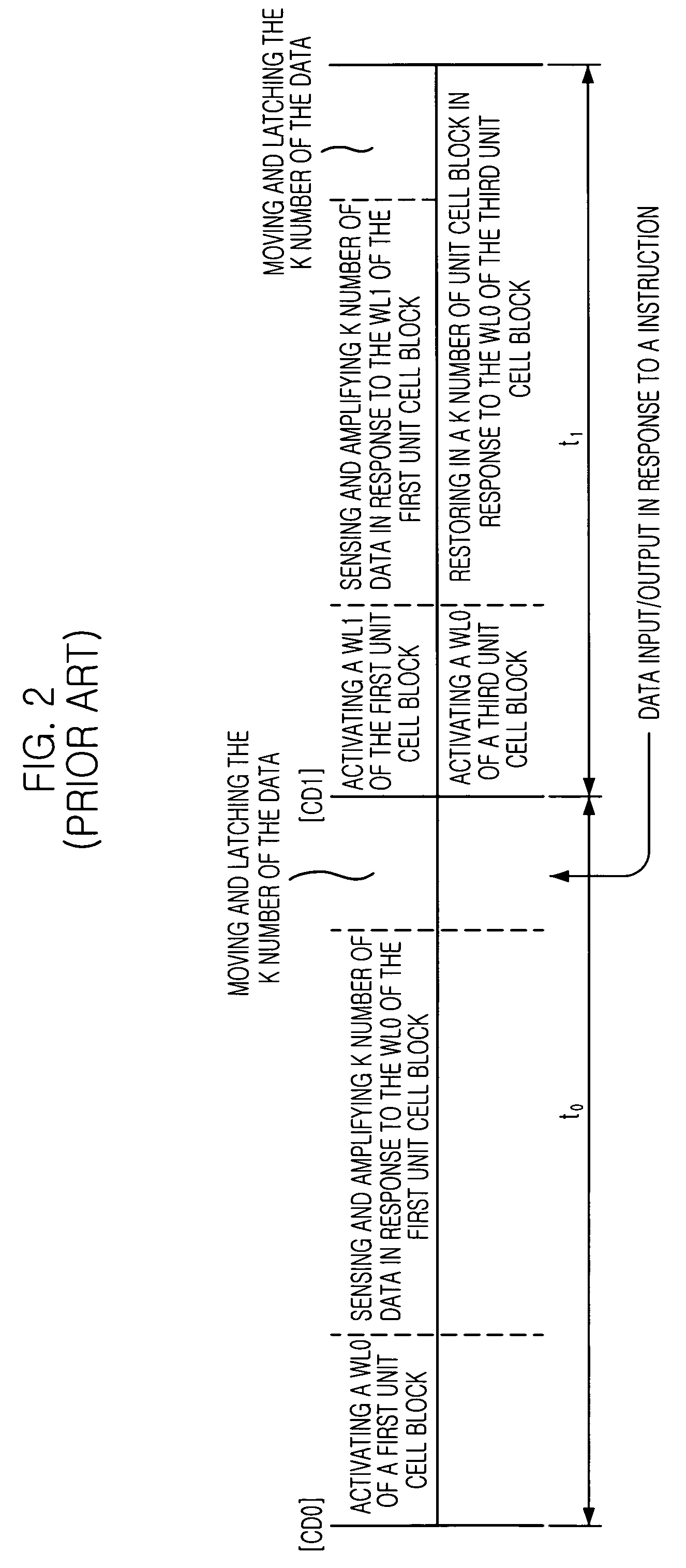
Accordingly, as seen in FIG. 1, if operation of the entire unit cell blocks is to be controlled with one controlling unit, circuit configuration of the controlling unit becomes so complicated, which will lead an obstacle to the high speed operation.

Method used


Image

  • Semiconductor memory device for controlling cell block with state machine
  • Semiconductor memory device for controlling cell block with state machine
  • Semiconductor memory device for controlling cell block with state machine

Examples

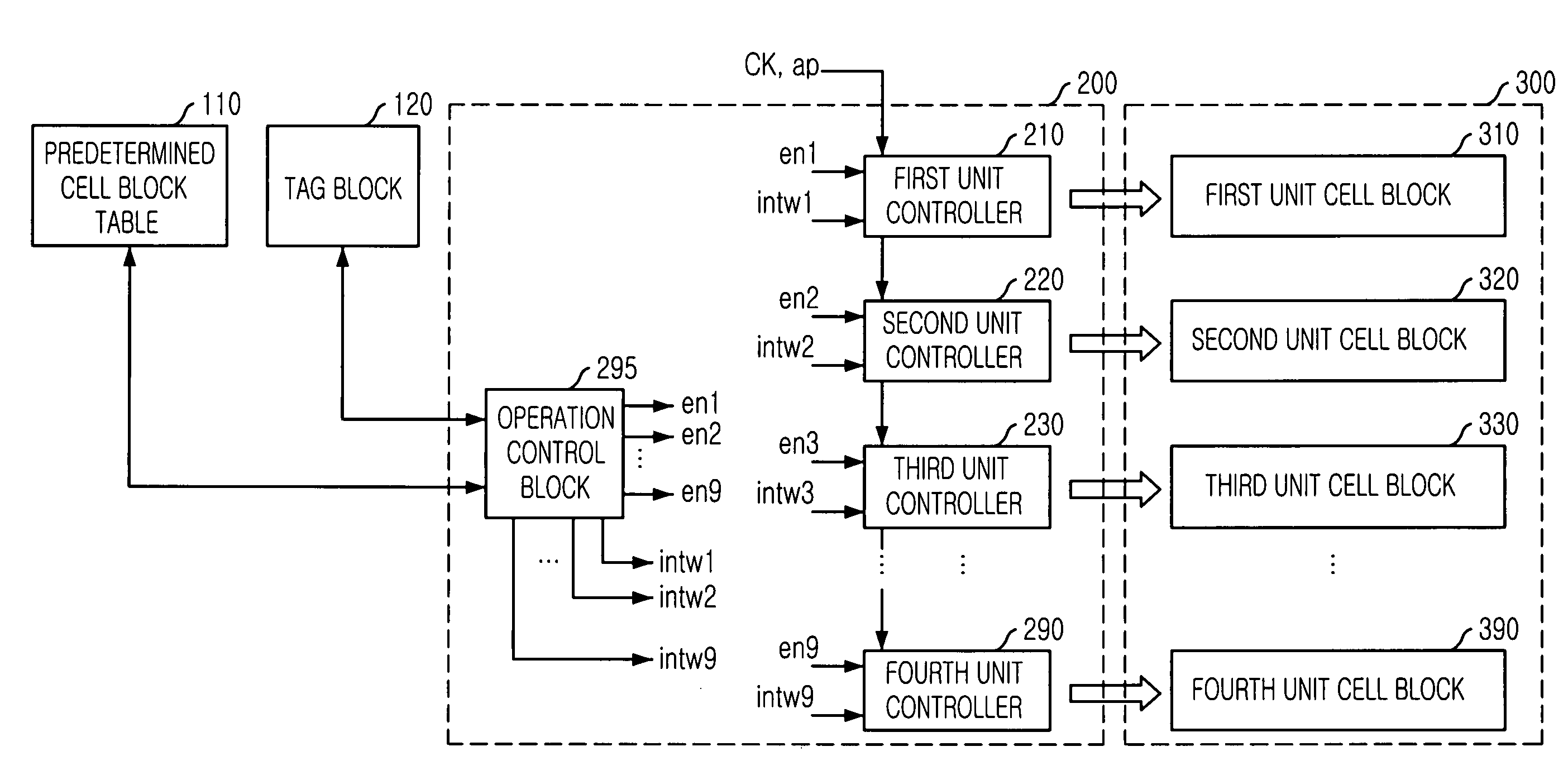

Embodiment Construction

[0025]Hereinafter, a semiconductor memory device in accordance with the present invention will be described in detail referring to the accompanying drawings.

[0026]FIG. 3 is a block diagram showing a semiconductor memory device in accordance with a preferred embodiment of the present invention.

[0027]Referring to FIG. 3, the memory device of the present invention includes a cell block 300 including 8+1 unit cell blocks, each having 256 word-lines, the 9 unit cell blocks including the 8 unit cell blocks corresponding to an inputted row address and an additional unit cell block, and a controlling unit 200 including 8+1 unit controlling units 210–290 and a driving controlling unit 295, the 8+1 unit controlling unit having respective state machines and corresponding to respective 8+1 unit cell blocks, for controlling to restore data that is accessed from a first unit cell block selected from the 8+1 unit cell blocks into the first unit cell block or a second unit cell block different from...


PUM


Abstract

A semiconductor memory device for an effective data access operation includes a cell area having N+1 number of unit cell blocks, each including M number of word lines, for storing a data in a unit cell corresponding to an inputted address; N+1 number of unit controlling blocks having respective state machines and corresponding to the respective N+1 unit cell blocks for controlling a data restoration that is accessed from a first unit cell block selected from the N+1 unit cell blocks into the first unit cell block or a second unit cell block; and a driving controlling block for controlling the N+1 unit cell blocks so that the N+1 unit controlling means are in one of first to fourth operation states.

Description

FIELD OF INVENTION[0001]The present invention relates to a semiconductor memory device; and, more particularly, to a semiconductor memory device for controlling a cell block with a state machine.DESCRIPTION OF PRIOR ART[0002]Recently, operational speed of a CPU has been improved even beyond operational speed of a memory device such as DRAM. Such slower operational speed of the memory device than the CPU leads some problems. In order to resolve those problems, various structures of the memory device are developed to input / output data at a higher speed.[0003]FIG. 1 is a block diagram showing a conventional semiconductor memory device disclosed in a commonly owned copending application, U.S. Ser. No. 10 / 696,144, filed on Oct. 28, 2003, entitled “SEMICONDUCTOR MEMORY DEVICE WITH REDUCED DATA ACCESS TIME”, which is incorporated herein by reference.[0004]Referring to FIG. 1, the memory device having high-speed data access capabilities includes a cell block 500 that is formed with 9 unit c...

Claims


Application Information

Patent Timeline
Patent Type & Authority Patents(United States)
IPC IPC(8): G11C8/00G11C7/10G11C7/22G11C8/12G11C29/00
CPCG11C8/12G11C7/22G11C7/10
Inventor HONG, SANG-HOONKO, JAE-BUMKIM, SE-JUN
Owner SK HYNIX INC
Learn More