Scan structure in display device, method for driving the display device, and method for manufacturing the same

a display device and structure technology, applied in the field of display devices, can solve the problems of deteriorating image uniformity, increasing the size of the device, and complicated system, and achieve the effects of reducing the duty in half, ensuring uniform picture quality, and convenient driving

Inactive Publication Date: 2006-06-27
LG DISPLAY CO LTD
View PDF18 Cites 4 Cited by
  • Summary
  • Abstract
  • Description
  • Claims
  • Application Information

AI Technical Summary

Benefits of technology

[0034]An object of the present invention is to provide a scan structure in a display device for physically decreasing a duty in half, maintaining uniform picture quality, and easy driving; a method for driving the display device; and a method for manufacturing the same.
[0035]Another object of the present invention is to provide a scan structure in a display device for physically decreasing a duty in half without increasing a size of a driver IC compared with dual-scan structure and dividing a panel; a method for driving the display device; and a method for manufacturing the same.

Problems solved by technology

In this respect, the LCD devices are generally used in monitors for portable information terminals due to less power consumption even though the LCD devices have disadvantages in a response time, a viewing angle and a color depth, as compared to other flat panel displays.
First, a plurality of data drivers is formed in the display device, so that a size of the device is increased, and the system is complicate.
Accordingly, a current difference may be generated between two parts, thereby deteriorating uniformity of image.

Method used


Image

  • Scan structure in display device, method for driving the display device, and method for manufacturing the same
  • Scan structure in display device, method for driving the display device, and method for manufacturing the same
  • Scan structure in display device, method for driving the display device, and method for manufacturing the same

Examples


first embodiment

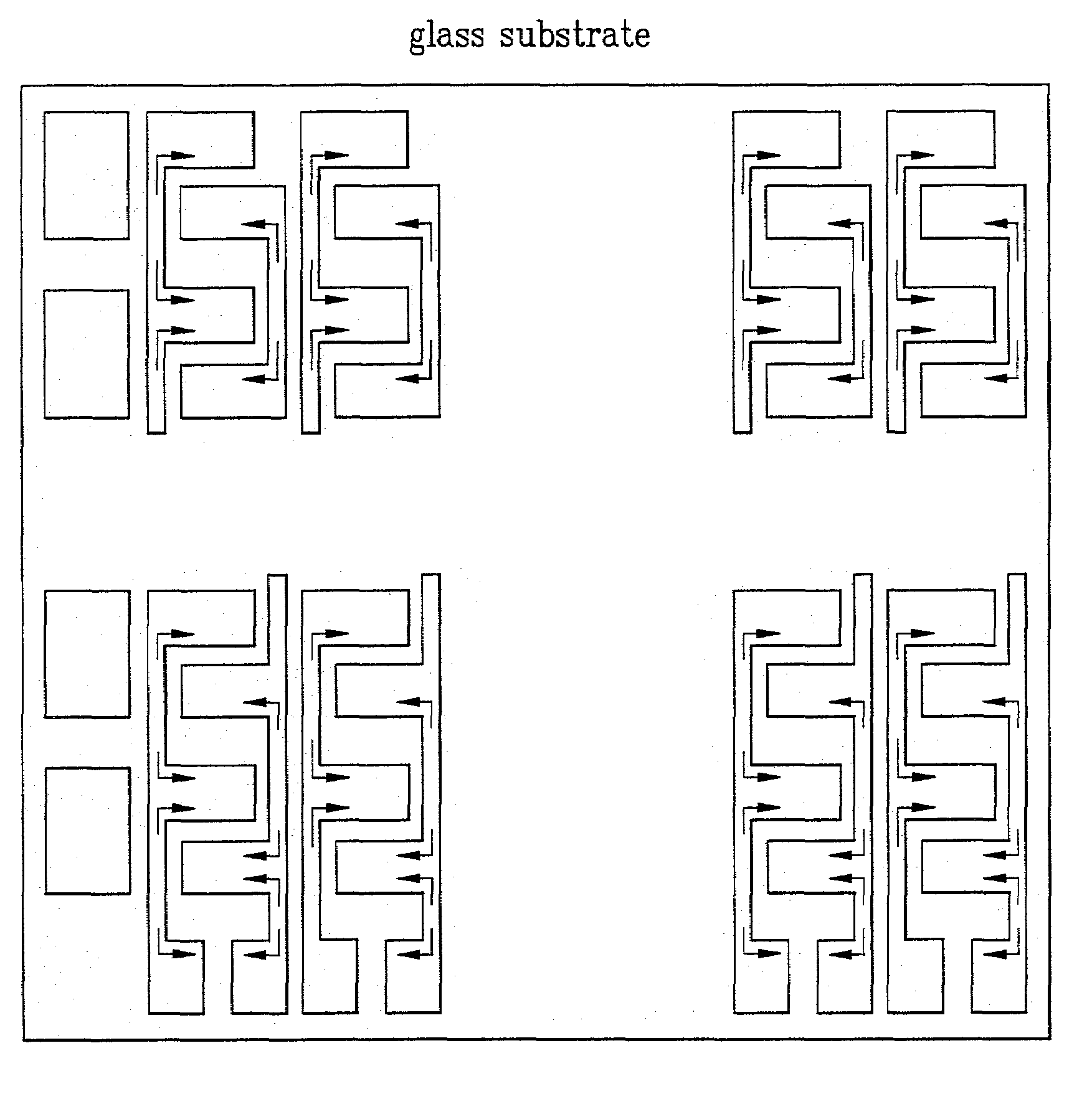
[0054]FIG. 3 is a view showing a scan structure of a display device according to the present invention.

[0055]As shown in FIG. 3, the display device according to the present invention includes an organic EL panel 200, a data driver 20 and a scan driver 10.

[0056]At this time, a plurality of data lines 60 and scan lines 50a are formed in a matrix type on the organic EL panel 200. That is, the plurality of data lines 60 cross the plurality of scan lines 50a, thereby forming a plurality of pixels (units for emitting lights) of the organic EL panel 200. Then, the data driver 20 and the scan driver 10 selectively apply currents to the data and scan lines 60 and 50a, so that light is selectively emitted from the pixels of the organic EL panel 20.

[0057]In the organic EL panel 200, a unit scan line 50a is formed of two scan lines. In this respect, a width of the unit scan line 50a is increased, so that a resistance of the unit scan line 50a is decreased.

[0058]In the above organic EL panel 200...

second embodiment

[0067]FIG. 4 is a view showing a scan structure of a display device according to the present invention.

[0068]As shown in FIG. 4, the display device includes an organic EL panel 200, a data driver 20 and a scan driver 10.

[0069]At this time, a plurality of data lines 60 and scan lines 50b are formed in a matrix type on the organic EL panel 200. Then, the data driver 20 and the scan driver 10 apply signals to the data and scan lines 60 and 50b, so that light is selectively emitted from the organic EL panel 20.

[0070]In the organic EL panel 200, two scan signals are simultaneously applied from the scan driver 10 to the scan lines 50b. That is, the first scan signal is simultaneously applied to the first and second scan lines, and then the second scan signal is simultaneously applied to the third and fourth scan lines.

[0071]Like FIG. 3, one data line serves to connect supplemental metal electrodes corresponding to even numbered scan lines with one another, and the other data line serves t...


PUM

PropertyMeasurementUnit
frame frequencyaaaaaaaaaa
frequencyaaaaaaaaaa
scan structureaaaaaaaaaa

Abstract

A scan structure of a display device, a method for driving the display device, and a method for manufacturing the same is disclosed, which is for physically decreasing a duty in half, maintaining uniform picture quality. In the display device having a plurality of data lines formed in one direction, a plurality of scan lines formed in perpendicular to the plurality of data lines, a plurality of pixels are formed, which are connected to the plurality of data lines in each scan line, so that the total scan time is increased in proportion to the number of the pixels in each scan line.

Description

[0001]This application claims the benefit of the Korean Application No. P2001-24360 filed on May 4, 2001, which is hereby incorporated by reference.BACKGROUND OF THE INVENTION[0002]1. Field of the Invention[0003]The present invention is related to a display device, and more particularly, to a scan structure in a display device for decreasing a duty at a passive panel, a method for driving the display device, and a method for manufacturing the same.[0004]2. Discussion of the Related Art[0005]Recently, flat panel displays have been rapidly developed. In especial, the flat panel display such as a liquid crystal display (LCD) device substitutes for a cathode ray tube (CRT). Also, the flat panel displays such as a plasma display panel (PDP), a vacuum fluorescent display (VFD), a field emission display (FED), a light emitting diode (LED) and an electroluminescence (EL) are being actively researched.[0006]The flat panel displays can be used in various fields in that the flat panel displays...

Claims


Application Information

Patent Timeline
Patent Type & Authority Patents(United States)
IPC IPC(8): G09G5/00G02F1/133G09F9/30G09G3/20G09G3/30G09G3/32H01L27/32H01L51/50H05B33/10H05B33/26
CPCG09G3/3216H01L27/3288G09G2310/0205G09G2300/0439H10K59/179G09G3/20
Inventor KIM, HAK SU
Owner LG DISPLAY CO LTD
Why Eureka
Try Eureka