Surface mount crystal unit and surface mount crystal oscillator
- Summary
- Abstract
- Description
- Claims
- Application Information
AI Technical Summary
Benefits of technology
Problems solved by technology
Method used
Image
Examples
first embodiment
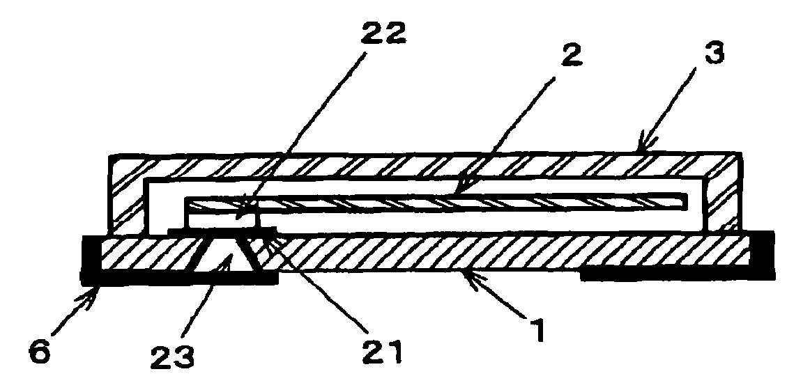
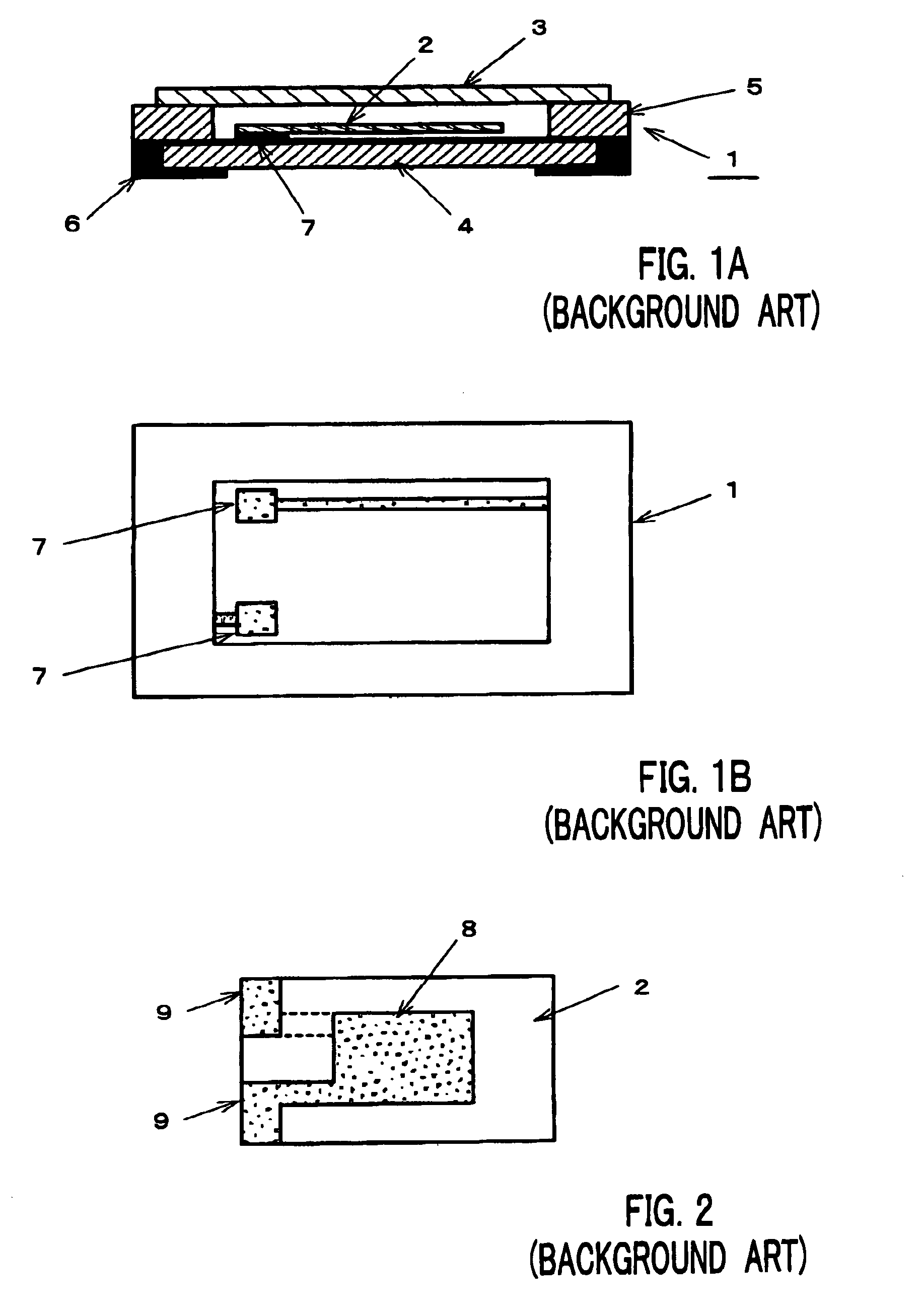
[0047]The surface mount quartz crystal unit according to the present invention shown in FIGS. 5A to 5C comprises quartz crystal blank 2 hermetically sealed in a case made up of substantially square planar mounting substrate 1 and cover 3 having a shape with a recess. As crystal blank 2, the one described in FIG. 2 is used.
[0048]Mounting substrate 1 is made up of a silicon (SI) substrate. Two metal films 21 are provided close to one short side on the surface of mounting substrate 1. The direction of the line connecting the two metal films 21 is parallel to the direction in which the short side of mounting substrate 1 extends. A small piece of metal plate 22 is bonded to each metal film 21 by means of silver solder or the like. Metal plates 22 are arranged on the positions which correspond to opposite sides of one end crystal blank to extension electrodes are extended. Crystal blank 2 is electrically and mechanically connected to mounting substrate 1 by connecting opposite sides of on...
second embodiment
[0071]In the crystal unit in the above described second embodiment, the positions at which through-holes 23 are formed are not limited to the ones described above. Considering that polycrystalline-silicon is also subject to anode bonding, as shown in an enlarged view in FIG. 9, it is also possible to form through-holes 23 at the position at which cover 3 and mounting substrate 1 are bonded, provide polycrystalline-silicon layers 24 so as to extend from the position at which through-holes 23 is formed to the inside of the case and connect crystal blank 2 at the position at the end of polycrystalline-silicon layers 24 through bump 25. Thus, providing through-holes 23 at the bonding positions of anode bonding can further assure airtightness.
[0072]Furthermore, the positions of mounting terminals 6 on the outer surface of mounting substrate 1 are not limited to the above described positions. It is possible to form polycrystalline-silicon layer 24 as a conductor path, form mounting termin...
third embodiment
[0076]Then, the present invention will be explained. The surface mount crystal unit of the above described embodiments functions as a surface mount crystal oscillator by incorporating an IC chip in which an oscillation circuit using the crystal blank is integrated. In the example shown in FIG. 7, such an IC chip is placed in a space between the crystal blank and mounting substrate. However, since the IC chip uses a silicon semiconductor substrate per se, the mounting substrate made of silicon itself can be used as an IC chip. The mounting substrate provided with the function as an IC chip makes it possible to reduce the number of constituent elements, external dimensions, especially height in the surface mount crystal oscillator.
[0077]The surface mount crystal oscillator according to the third embodiment shown in FIGS. 11A and 11B comprises crystal blank 2 hermetically sealed in a case made up of substantially square planar mounting substrate 30 and cover 3 having a shape with a rec...
PUM
 Abstract
Description
Claims
Application Information
 - R&D
- Intellectual Property
- Life Sciences
- Materials
- Tech Scout
- Unparalleled Data Quality
- Higher Quality Content
- 60% Fewer Hallucinations
Browse by: Latest US Patents, China's latest patents, Technical Efficacy Thesaurus, Application Domain, Technology Topic, Popular Technical Reports.
© 2025 PatSnap. All rights reserved.Legal|Privacy policy|Modern Slavery Act Transparency Statement|Sitemap|About US| Contact US: help@patsnap.com


