Device and method for associating information concerning memory cells of a memory with an external memory

a technology of memory cells and memory elements, applied in the field of devices and methods for associating information concerning memory cells in memory elements with external memory, can solve problems such as unnecessarily high fault memory demand, and achieve the effects of reducing the effective demand of fault memory, and reducing the size of address spa

Inactive Publication Date: 2006-03-28
POLARIS INNOVATIONS LTD
View PDF2 Cites 0 Cited by
  • Summary
  • Abstract
  • Description
  • Claims
  • Application Information

AI Technical Summary

Benefits of technology

[0016]An advantage of the present invention thus consists in a reduction of the effective demand of fault memory in testing a memory element and in particular in checking redundant cells. Thus, in testing a memory element, the invention, for example, successfully achieves, by way of a circuit, a reduction of size of the address space by increasing the number of data outputs, without interfering with the normal function of the DRAM, with the increase in the number of data outputs not taking place in the same ratio as the reduction of address space. The device or circuit according to the invention can be realized externally, e.g. by an ASIC (Application Specific Integrated Circuit) that is mounted on a probe card or is a constituent part of a memory testing system. In that case, there are no changes whatsoever necessary to the DRAM. As an alternative, such a circuit may be integrated in the DRAM, and use thereof may be controlled via a test mode. In this case too, there is no change to the cell field architecture necessary.
[0017]A device or circuit according to the present invention has n inputs and m>n, m<2n outputs and may be operated in a buffer mode and in an output mode. In the buffer mode, the n input data are filed in an addressable intermediate memory or buffer means. The memory cells are selected in accordance with address bits applied. In the output mode, the n inputs are connected through to the first n outputs. The contents of the buffer memory is output in parallel via the remaining m−n outputs, with the respective datum being selected in accordance with addresses applied. The assignment between address bits applied and cells of the buffer memory is programmable and may differ in the buffer mode and in the output mode.
[0018]Further developments of the present invention are defined in the dependent claims.

Problems solved by technology

This is disadvantageous if the aforementioned testing of the operability of all memory cells of a memory element is carried out with test systems as they are usual in the market, making use of a fault memory of a size corresponding to the effective address space.
Consequently, there is arising an unnecessarily high fault memory demand.

Method used


Image

  • Device and method for associating information concerning memory cells of a memory with an external memory
  • Device and method for associating information concerning memory cells of a memory with an external memory
  • Device and method for associating information concerning memory cells of a memory with an external memory

Examples


Embodiment Construction

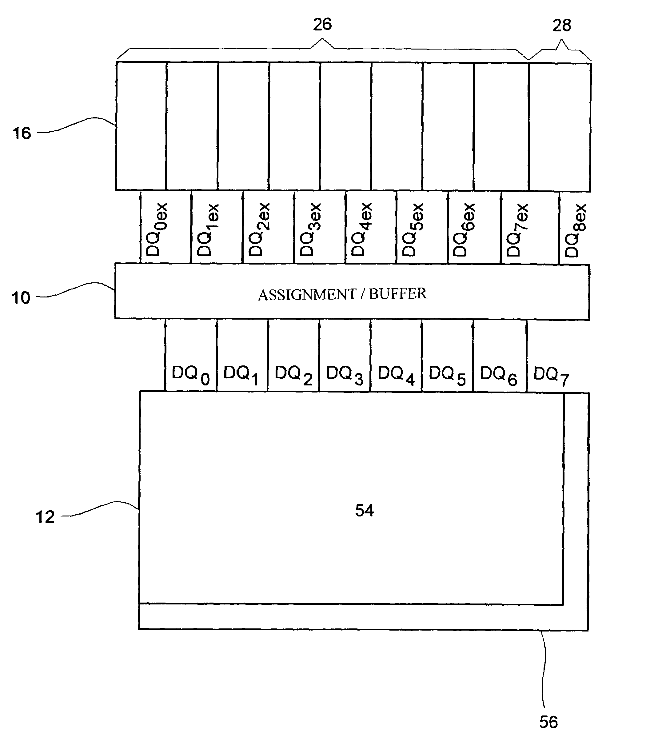
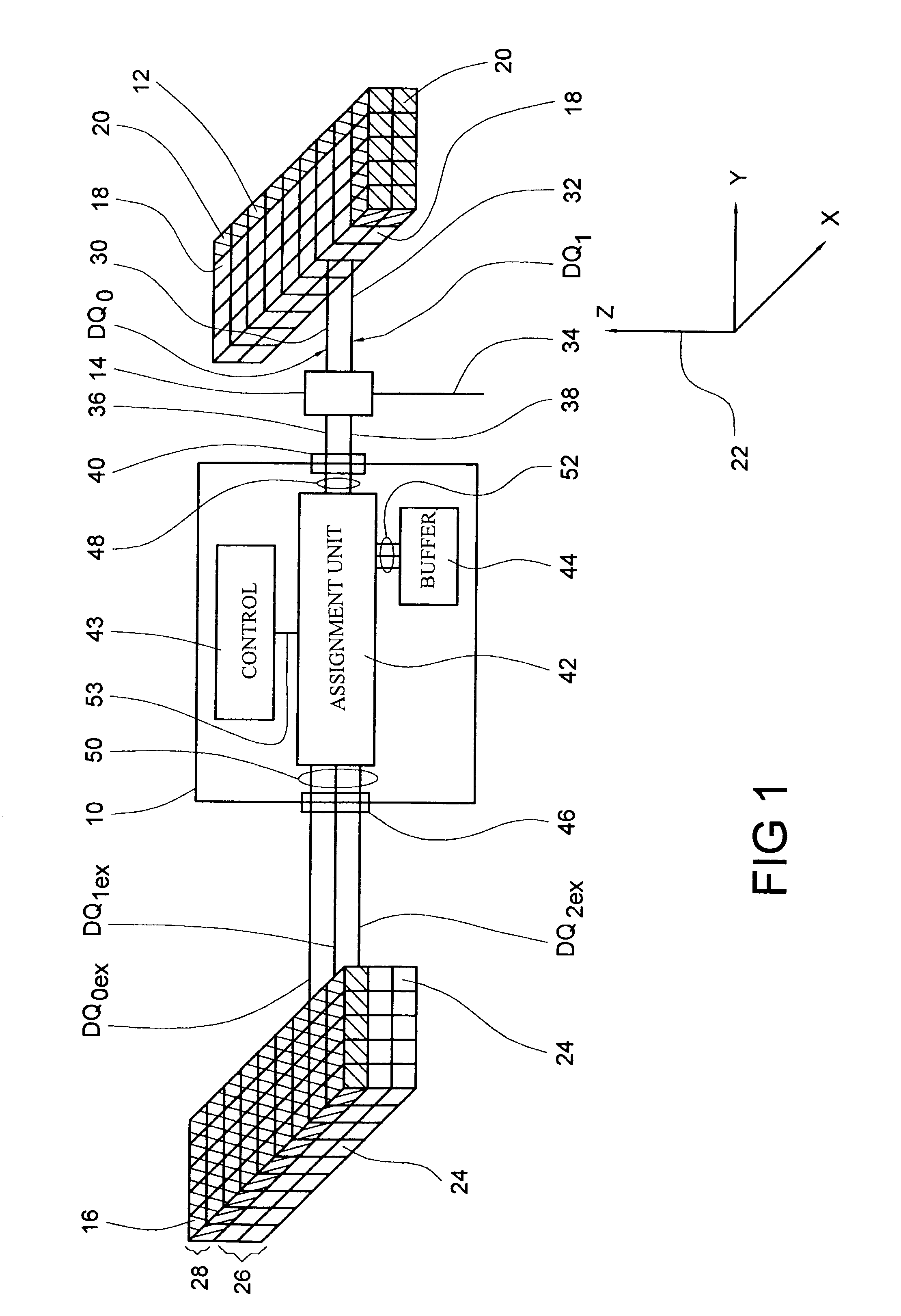
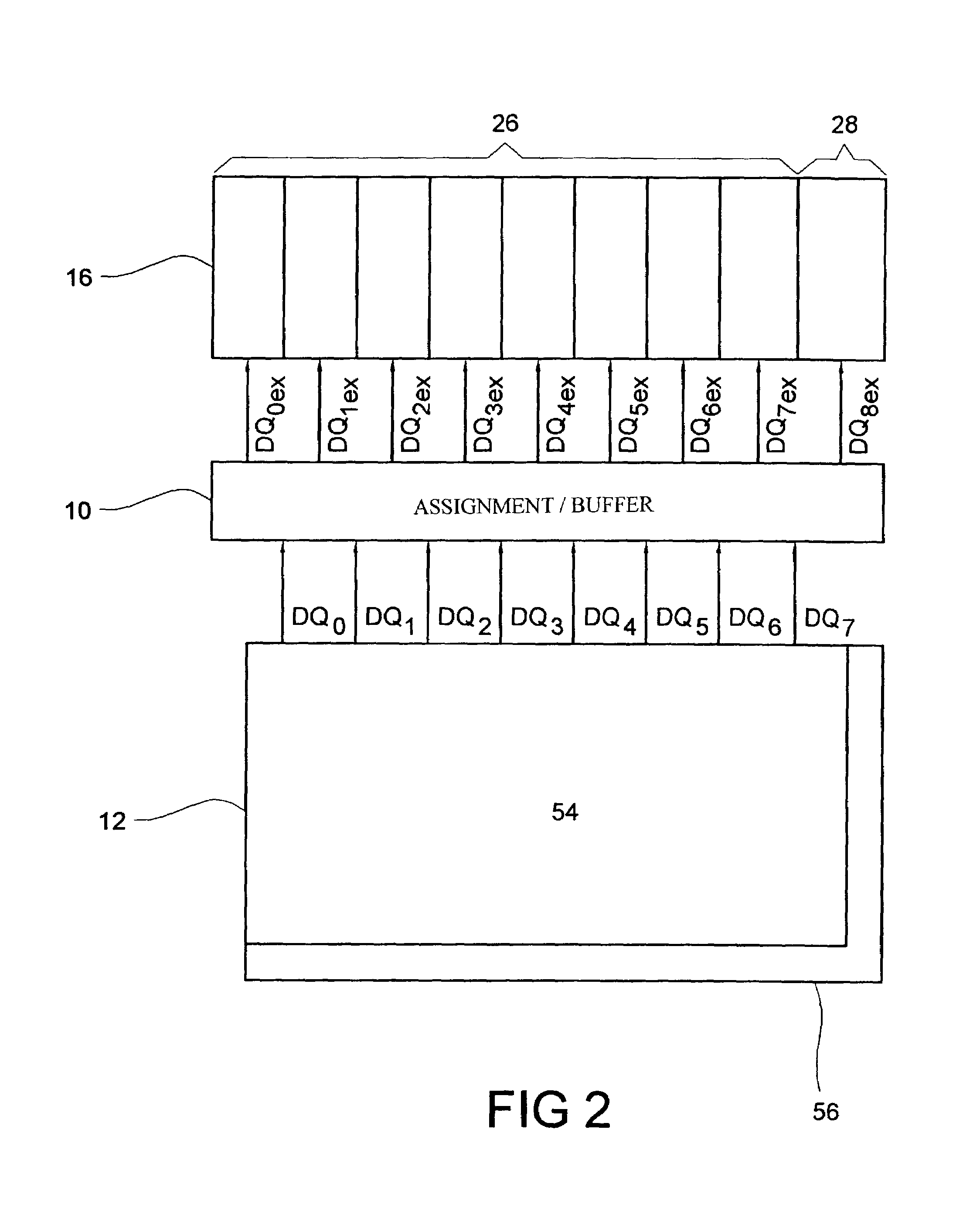
[0023]FIG. 1 illustrates a schematic representation of a preferred embodiment of the present invention. The device 10 according to the invention is illustrated together with a memory element 12, a comparator 14 and a fault memory 16.

[0024]The memory element 12 comprises first memory cells 18 (shown in white color in FIG. 1) and second memory cells 20 (shown in hatched manner in FIG. 1). For keeping a clear illustration, only some of the memory cells in FIG. 1 bear reference numerals.

[0025]The first memory cells 18 are arranged in a regular portion of the memory element 12, preferably in matrix form, in four columns and eight rows. In order to more clearly illustrate the directions, FIG. 1 schematically shows a coordinate system 22. The columns are arranged adjacent each other in y direction and extend in x direction. The rows are arranged adjacent each other in x direction and extend in y direction. The arrangement just described relates to addressing by means of a column address (h...


PUM


Abstract

In a device and a method associating information concerning first memory cells and second memory cells of a memory element with an external memory, with each address of the memory element having a first predetermined number of memory cells associated therewith and each address of the external memory having a second number of memory cells associated therewith that is greater than said first predetermined number, and with said second predetermined number of memory cells on each address of the external memory being adapted to be subdivided into a first group of memory cells and a second group of memory cells, an input receives the information concerning said first and second memory cells. The information concerning first memory cells is assigned to the first group of memory cells in the external memory, and the information concerning the second memory cells is associated to the second group of memory cells in the external memory. Via an output adapted to be connected to the external memory, the information concerning the memory cells of the memory element is output to the associated group in the external memory.

Description

BACKGROUND OF THE INVENTION[0001]1. Field of the Invention[0002]The present invention relates to a device and a method for associating information concerning memory cells in a memory element with an external memory, and in particular to a device and a method for associating fault information in testing the memory element with the external memory and for filing the information in the same.[0003]2. Description of the Related Art[0004]Dynamic semiconductor memories, such as e.g. DRAMs (DRAM=Dynamic Random Access Memory), as a rule have additional, redundant memory cells apart from a number of memory cells in a regular portion which corresponds to the nominal size of the semiconductor memory. Upon manufacture of a semiconductor memory, all memory cells are tested with respect to operability thereof and defective memory cells in the regular portion are replaced by operable redundant memory cells by re-addressing. The replacement of the memory cells as a rule does not take place individua...

Claims


Application Information

Patent Timeline
Patent Type & Authority Patents(United States)
IPC IPC(8): G06F12/00G11C7/10G11C29/00G11C29/56
CPCG11C7/1045G11C7/1051G11C7/1057G11C7/1078G11C29/56G11C7/1084G11C2029/5606G11C11/401G11C29/70G11C2029/1806
Inventor RIEGER, MARTIN
Owner POLARIS INNOVATIONS LTD
Why Eureka
Try Eureka